

CoaXPress Acquisition Demo Based on RFSOC FPGA ZCU216
1.Background
The customer needs to use RFSCOC to implement CoaXPress image acquisition and processing, and then control the RFSOC DAC for sequence signal output. The RFSCOC development platform selected is the Xilinx ZCU216.
The ZCU216 is an evaluation board equipped with the ZU49DR device from the AMD Zynq™ UltraScale+™ RFSoC Gen3 series. This board can be used to evaluate applications for sub-6 GHz band radios, millimeter-wave, as well as complete L-band and S-band applications in phased array radar. The ZCU216 board is equipped with various board-level features required for design and development, including DDR4 memory, network interfaces, FMC+ expansion interfaces, and RFMC 2.0 interface access capability.
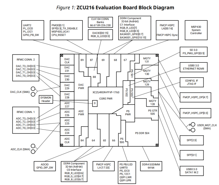
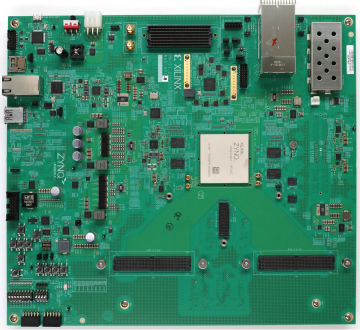

Fig. 1-1 FMC-CXP-4R CoaXPress 2.0 Daughter Card
FMC-CXP-4R 4-Channel CoaXPress FMC Daughter Card - Chongqing Xingce Electronic Technology Co., Ltd.
2.Hardware Preparation
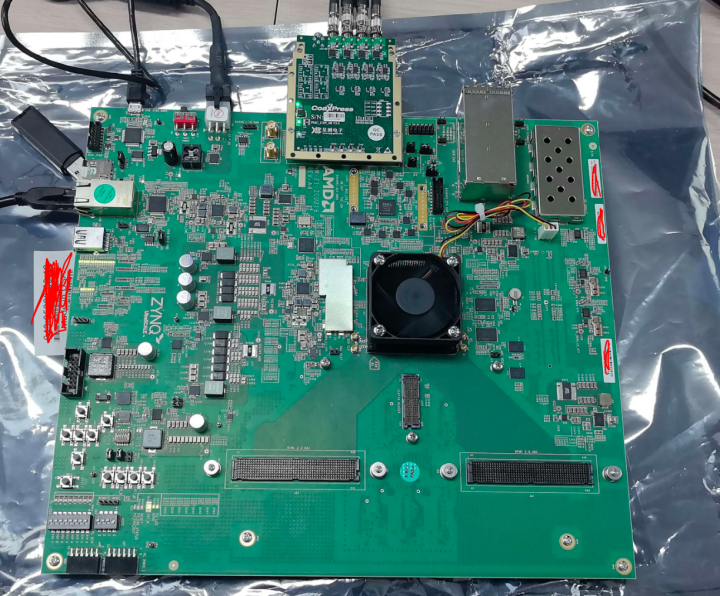
- Xilinx ZCU216 board
- Xingce Electronics FMC-CXP-4R
- MIKROTRON's 25CXP+ high-speed CMOS cameras / Hamamatsu qcmos C15550-22UP
- ImgGrab Chongqing Xingce Electronic Technology Co., Ltd. - Download , latest version recommended
3.Test Steps
- Set the ZCU216 to SD card boot mode.
- Install the SD card image on the ZCU216 (contact Xingce Electronics to obtain).
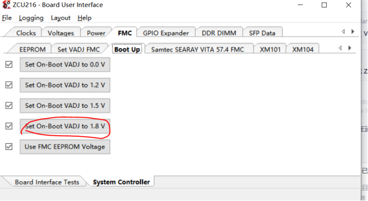
- Set the FMC VADJ power-on startup voltage to 1.8 V in advance on the ZCU216. By default, FMC VADJ does not output voltage; it needs to read the daughter card information via IIC first and then decide which voltage level to use. The IIC of the FMC-CXP-4R uses VADJ for level shifting, which creates a contradiction. Setting the startup voltage level at boot resolves this, and no further configuration is needed afterwards.
- Make the hardware connections. Before powering on, connect the FMC-CXP-4R daughter card to the camera, connect the Ethernet cable to the ZCU216, and ensure it is on the same LAN as the Windows PC. It is recommended to connect both to the LAN so that DHCP is automatically assigned. Users can scan for the corresponding ZCU216 device via serial port or ImgGrab. Currently, the Gigabit Ethernet is only used for image preview, not for real-time image transmission. Users can perform ISP image processing directly on the ZCU216, while previewing and collecting result data on Windows and other clients.
- Power on the device to enter the PYNQ system. The default username is xilinx and the password is also xilinx. Users can access it via serial port, SSH, or Notebook.
- Open ImgGrab to automatically scan for ZCU216 and camera devices. If anything is unclear, please refer to the manual at https://img-grab.com/productinfo/306297.html and the ImgGrab User Guide.
- If users modify the FPGA program, note that the existing module address allocation must not be changed. The generated bit file after modification needs to replace /home/xilinx/overlays/cxp_host_wrapper.bit.
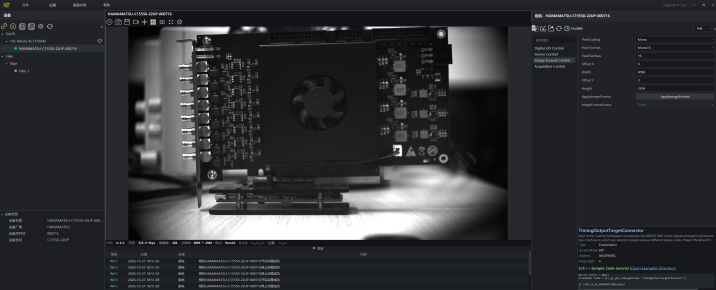
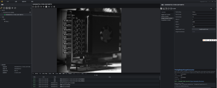
This is the test video, showing the hardware connections and software operation demonstration.
https://www.bilibili.com/video/BV14Vxx6SEDR/
https://www.bilibili.com/video/BV1tGxx6nEvX/
4.FPGA Secondary Development Instructions
- Vivado 2022.2
- PetaLinux 2023.1 (or a newer version). PYNQ has already been built and can be used directly.
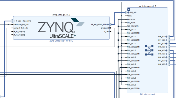
The Zynq PS serves as the main controller, running the PYNQ operating system and booting from the SD card.
If users modify the FPGA program, note that the existing module address allocation must not be changed. The generated bit file after modification needs to replace /home/xilinx/overlays/cxp_host_wrapper.bit.
5.SDK Secondary Development Instructions
Chongqing Xingce Electronic Technology Co., Ltd. - Download
FrameGrabber_SDK_Examples contains software SDK secondary development examples, which users can develop on Windows.


