FMC-CXP-4T
● Channels: 4 CoaXPress transmitting links
● Data Rate: Max 12.5Gbps per channel, 50Gbps aggregated bandwidth across four channels
● Equalizer: CXP12EQCO125X40 high-speed equalizer with integrated CDR
● Connectors: FMC HPC (VITA57.1), 4× HD BNC, 1× SMA
● Onboard Storage: 2Kb MT24C02 I2C EEPROM (256 Bytes)
● Designed for CXP image simulation and camera prototyping, suitable for testing and verification of all CXP frame grabbers
FMC-CXP-4T 4-Channel CoaXPress FMC Card
High-Speed CXP Data Transmission & Camera Emulation Module
- Supports CXP12 / HDBNC / SMA Trigger

4 Core Advantages
CXP12 Full-Rate Transmission
Supports CoaXPress 2.0 protocol, single-channel rate up to 12.5Gbps, 4-channel aggregate bandwidth 50Gbps. Compatible with CXP-1 to CXP-12 rates, ideal for high-speed data transmission and camera emulation.
High-Speed Signal Equalization
Integrates CXP12EQCO125X40 high-speed equalizer with built-in Clock Data Recovery (CDR). Cable transmission distance up to 35m at 12.5Gbps, ensuring signal integrity and stability.
HDBNC + SMA Dual Interface
Equipped with 4x HD BNC high-speed interfaces (compatible with standard CoaXPress coax cables) and 1x SMA bi-directional trigger interface (3.3V TTL, ±24mA drive), meeting multi-scenario trigger and synchronization needs.
Wide FMC HPC Compatibility
Adopts HPC FMC connector (VITA57.1 standard), compatible with all FMC HPC FPGA carrier boards and full-series Xilinx FPGAs. Paired with HelloFPGA-KU5P to build cost-effective CXP prototypes.
Introduction to CoaXPress Protocol
- CoaXPress is an asymmetric high-speed point-to-point serial standard that transmits image data, control signals, and power over a single coaxial cable, featuring high real-time performance, fixed latency, and strong anti-interference.
- Single-channel rate up to 12.5Gbps, 4-channel aggregation 50Gbps. Supports RG59/RG6 cables: 100m at 3.125Gbps, 35m at 12.5Gbps.
- Supports precise real-time trigger via coaxial cable (no extra wiring). Integrated power delivery simplifies system wiring with one cable for power, data, and control.
Product Features
- FMC-CXP-4T is a 4-channel CoaXPress FMC card designed for CXP image emulation and camera prototyping, supporting up to 4-channel CXP-12 full-rate data transmission for CXP frame grabber testing and validation.
- Emulates CXP camera operation: high-speed image data transmission, control signal interaction, and trigger response, providing flexible prototyping for CXP acquisition system development.
- FMC HPC connector (VITA57.1) compatible with full-series Xilinx FPGA carrier boards, enabling fast integration and reducing system development costs.
- Onboard 2Kb EEPROM (MT24C02) for custom configuration storage; dual-color LED per channel (programmable via FPGA I/O) for real-time status indication.
- Works with HelloFPGA-KU5P carrier to build cost-effective CXP prototypes for camera emulation, frame grabber testing, and industrial vision validation.
Hardware Specifications
- Channels: 4x CoaXPress transmit links, CXP-1 ~ CXP-12, 12.5Gbps/Ch, 50Gbps aggregate.
- Interfaces: 4x HD BNC (CXP signals), 1x SMA bi-directional trigger (3.3V TTL), 1x FMC HPC (VITA57.1).
- Signal Processing: CXP12EQCO125X40 equalizer with CDR, 8b/10b encoding for downlink transmission and uplink control reception.
- Trigger I/O: SMA bi-directional I/O, SN74LVC1T45 level shifter, FPGA-controlled direction, max 210Mbps rate.
- Extras: 2Kb EEPROM (I2C), 125MHz GT RefCLK, 4x dual-color LED indicators.
- Mechanical: Single-width FMC 63mm×84mm, industrial temp -40℃~85℃, high-speed PCB for signal integrity.
- Electrical: 3.3V I/O, VOH=2V (typ), VOL=0.8V (max), input 0~5.5V, propagation delay 1-6ns.
Technical Parameters
| Item | Specification |
|---|---|
| Protocol | CoaXPress 2.0, CXP-1 ~ CXP-12 |
| Channels | 4x CoaXPress Transmit Links |
| Data Rate | 12.5Gbps/Ch, 50Gbps Aggregate |
| Connectors | FMC HPC (VITA57.1), 4x HD BNC, 1x SMA |
| Trigger I/O | SMA Bi-Directional I/O, 3.3V TTL, 210Mbps Max |
| Level Shifter | SN74LVC1T45DPKR, ±24mA Drive |
| Equalizer | CXP12EQCO125X40 with CDR |
| Memory | 2Kb EEPROM (MT24C02, I2C, 256Bytes) |
| Clock | 125MHz GT RefCLK |
| Dimensions | 63mm×84mm (Single-Width FMC) |
| Temperature | Industrial (-40℃~85℃) |
| PCB | High-Speed PCB for CXP Signal Transmission |
| Compatibility | Xilinx FPGA Boards with FMC HPC |
| Indicators | 4x Dual-Color LEDs (1/Ch, Programmable R/G) |
Product Interface Diagram

Product Interface Definition
Mechanical Drawing

Standard FMC Size: 63mm×84mm
Functional Block Diagram

- Equalizer/Driver: Transmits high-speed downlink signals from FPGA GTs, receives low-speed control signals from frame grabbers, integrated CDR for signal integrity.
- HD BNC Interface: Connects to frame grabbers via Micro BNC per CoaXPress standard for high-speed data transmission.
- LED Indicator: Dual-color LED per channel, programmable via FPGA I/O to display working status (Tx, standby, fault, etc.).
- EEPROM: MT24C02 (I2C, 256Bytes) for storing custom configurations (Device ID, rate settings, etc.).
- SMA Trigger: Bi-directional digital I/O for trigger routing, FPGA-controlled direction, 3.3V TTL compatible.
- Reference Clock: 125MHz GT RefCLK provides stable clock for high-speed transceivers, ensuring timing accuracy.
Safety Warnings (Must Read)
- DO NOT plug/unplug with power on: Turn off and disconnect power before installation/removal to avoid permanent damage.
- ESD Protection: Use anti-static wristband to prevent electrostatic damage to components.
- Avoid Harsh Environments: No water, direct sunlight, strong EMI, or vibration during operation/storage.
- Standard Connections: Use certified CoaXPress cables for HD BNC; verify trigger level matching for SMA to avoid short circuits.
- Thermal Management: Ensure adequate heat dissipation; avoid prolonged high-load operation in high-temperature environments.
Quick Start Guide
- Hardware Connection: Insert FMC-CXP-4T into FMC HPC slot, secure screws. Connect CXP frame grabber via HD BNC and trigger device via SMA.
- Power Setup: Confirm stable power supply for FPGA carrier, no over-voltage or reverse polarity.
- Configuration: Set clock, data rate, and trigger mode via FPGA logic; save custom settings to EEPROM.
- Camera Emulation: Configure operating mode to emulate CXP camera data transmission and control response for frame grabber testing.
- Verification: Power on system, check LED status, validate data transmission and trigger functions.
- Expansion: Use FPGA logic or SMA trigger for multi-card synchronization and complex control.
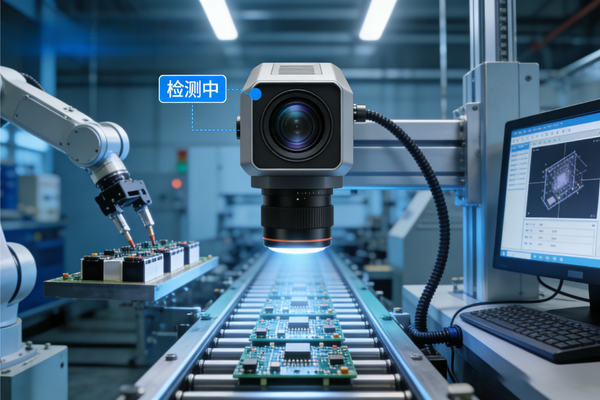
Typical Applications