


CameraLink FPGA FULL FMC
● Connectors: LPC FMC (VITA57.1 compliant), dual SDR26 ports
● Max Data Rate: 1.6 Gbps
● Signals: LVDS for data, single-ended for control
● GPIO Expansion: 30 channels (15 differential pairs), 2×18 pin headers with 2.54mm pitch
● Applications: Industrial vision, high-speed image acquisition
Hello-FPGA Camera Link Full
Receiver FMC Card
High-Speed Camera Link Image Acquisition Module - Supports Base/Medium/Full Modes

4 Core Advantages
Full Mode Compatibility
Fully supports Camera Link Base/Medium/Full configuration modes, direct LVDS connection to FPGA. Adapts to high-speed camera acquisition with bandwidth up to 1.6Gbps.
FMC LPC High-Efficiency Design
Adopts LPC FMC connector compliant with VITA57.1 standard, occupies fewer pins while ensuring stable high-speed data transmission for FPGA carrier boards.
Dual SDR26 Interfaces
Equipped with 2×SDR26 standard interfaces, compatible with Camera Link cables. Stable connection supports long-distance transmission for industrial applications.
Rich Expansion Capabilities
Provides 30-channel (15 differential pairs) GPIO expansion, supports 5V/12V output (5V max 2A drive), flexible for external device connection.
Introduction to Camera Link Protocol
- Camera Link is a serial communication protocol designed for industrial camera interfaces, standardizing connections for scientific and industrial video products.
- It uses Base/Medium/Full modes for different data throughput, LVDS synchronous timing for video data, serial ports for control data, and 4 LVDS IO pairs for trigger signals.
- With a maximum transmission rate of 1.6Gbps, it features high stability and anti-interference, widely used in industrial vision and high-speed imaging.
Hardware Features
- Supports Camera Link Base/Medium/Full modes, direct LVDS to FPGA, compatible with general LVDS applications.
- Mechanical size 69mm×82mm, single-width LPC FMC connector (VITA57.1 standard), compatible with mainstream FPGA carriers.
- Uses SDR26 connectors and cables for reliable high-speed transmission in industrial environments.
- Power output: 5V (max 2A), 12V (carrier-dependent), VADJ (carrier-dependent) for external devices.
- 30-channel (15 differential pairs) GPIO via 2×18 2.54mm header for function expansion.
- Comes with Hello-FPGA CL-PROBE-MDR26 adapter, converts MDR26 to screw terminals for easy testing.
Structure Description
- LPC FMC connector (VITA57.1 standard) for stable connection with FPGA carrier boards.
- Camera X/Y/Z data connects directly to FPGA IOs via MDR26 LVDS signals, low latency and high integrity.
- Camera control signals (CC1~CC4) and serial signals (SerTC/SerTCG) converted to single-ended by DS90LV031/DS90LV019 for FPGA control.
- Power system: 5V/12V/VADJ output, 5V max 2A drive for external equipment.
Technical Parameters
| Item | Specification |
|---|---|
| Protocol | Camera Link (Base/Medium/Full) |
| Connectors | LPC FMC (VITA57.1), 2×SDR26 |
| Data Rate | Up to 1.6Gbps |
| Signal Interface | LVDS (Data), Single-ended (Control) |
| GPIO | 30-ch (15 diff pairs), 2×18 2.54mm Header |
| Power Output | 5V (2A Max), 12V, VADJ |
| Dimensions | 69mm×82mm |
| Adapter Board | Hello-FPGA CL-PROBE-MDR26 (MDR26 to Screw Terminal) |
| Adapter Features | Matched Differential Lines, Clear Silkscreen, 100Ω Resistor Option |
| Operating Temp | Industrial (-40℃ ~ 85℃) |
Product Interface Diagram
Product Interface Definition
Mechanical Drawing
Front Size: 69mm×82mm
Debug Adapter (Hello-FPGA CL-PROBE-MDR26)
Hardware Features
- Integrates MDR26 and 3.81mm screw terminals with matched differential lines for signal integrity.
- Clear silkscreen marking for easy identification and wiring, reducing test complexity.
- Optional 100Ω differential resistor for flexible test scenarios.
- Custom-designed for Camera Link FMC card, plug-and-play.
Safety Warnings (Must Read)
- DO NOT plug/unplug the FMC card or adapter with power on. Turn off the carrier board to avoid ESD/short damage.
- Confirm power polarity and signal definition before wiring to prevent burnout. Use the official adapter for testing.
- Use ESD protection (wrist strap) during operation; precision components are sensitive to static electricity.
- Do not overload the 5V output (max 2A) to avoid overheating or damage.
- Avoid high humidity, strong EMI, and dusty environments for stable operation.
Quick Start Guide
- Hardware Connection: Insert the FMC card into the LPC slot of the FPGA carrier, secure with screws. Connect the adapter via MDR26 cable if needed.
- Power Check: Ensure the carrier board power is normal, and the 5V/12V loads are within limits.
- Signal Configuration: Select Camera Link mode (Base/Medium/Full) and configure GPIO/control signals via FPGA logic.
- Test Verification: Connect the Camera Link camera, power on the system, and verify data transmission with debug tools.
- Expansion: Connect external devices via GPIO and power interfaces following the user manual.
Typical Applications
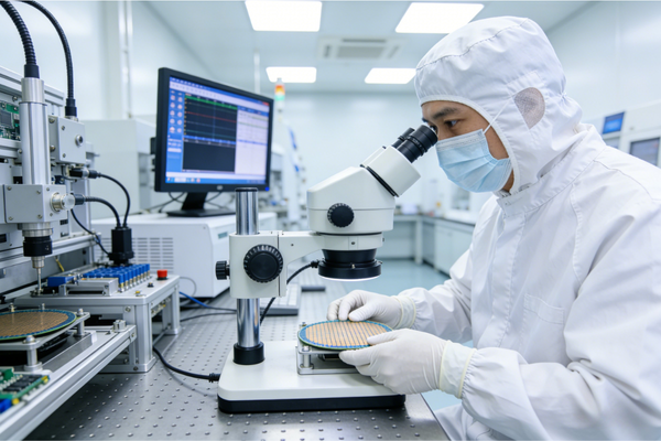
Semiconductor Inspection
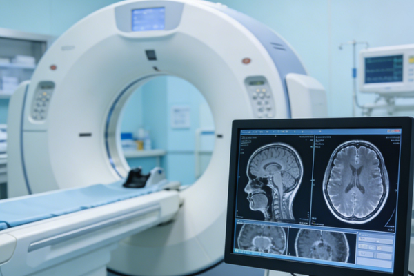
Medical Imaging

Aerospace
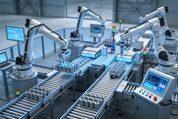
Industrial Automation
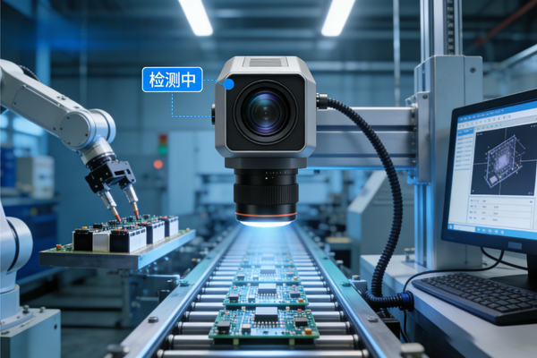
Machine Vision
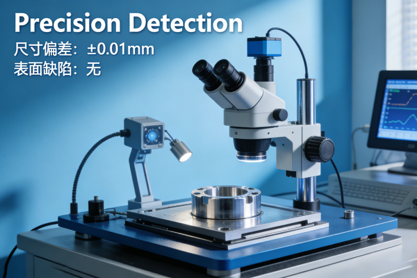
Precision Detection
