


Hello-FPGA-KU5P Development Board
● Memory Configuration: 2 GB DDR4 SDRAM (64-bit), 64 MB QSPI Flash
● Core Resources: 475K logic cells, 217K look-up tables (LUTs), 434K flip-flops, 1,824 DSP slices
● Interfaces: Supports high-speed SD card, MIPI and PCIe Gen3 x8 interconnection; equipped with Gigabit Ethernet port, UART and FMC HPC
● Applications: Industrial automation, intelligent vehicle systems, medical devices, aerospace and other fields
Hello-FPGA-KU5P FPGA Development Board
High-Performance Kintex UltraScale+ FPGA Platform - For High-Speed Data Exchange, Video Capture & Processing

4 Core Advantages
Powerful Programmable Logic Resources
Based on Xilinx XCKU5P-2FFVB6761 high-end chip, with 475K logic cells, 217K LUTs, 434K FFs, 1824 DSP multipliers and 16.9Mb Block RAM, meeting complex algorithm implementation and high-speed data processing requirements.
Multi-Protocol High-Speed Interconnection
Supports high-speed SD Card/MIPI/PCIe Gen3 x8 interconnection, equipped with Gigabit Ethernet, UART, FMC HPC interface. PCIe single-channel rate up to 8Gb/s, adapting to various high-speed peripherals and data transmission scenarios.
Flexible Hardware Expansion
Integrates 1x FMC HPC interface, 1x MIPI camera interface, 40PIN general expansion port, compatible with HDMI modules, high-speed AD modules and other peripherals, suitable for multi-scenario development and flexible module matching.
Large-Capacity Onboard Storage
Onboard 2GB DDR4 SDRAM and 64MB QSPI FLASH, equipped with 200Mhz differential clock for DDR4 driving, satisfying system operation, data caching and program storage, ensuring stable performance.
Product Overview
- Hello-FPGA-KU5P is a professional Kintex UltraScale+ FPGA development platform, designed for high-speed data exchange, video transmission & processing, industrial control and AI applications. Adopts 14-layer industrial-grade PCB with independent power and GND layers for excellent stability and reliability.
- Powered by Xilinx XCKU5P-2FFVB6761 chip, integrated with 16-channel 28Gb/s GTY high-speed transceivers, delivering powerful hardware acceleration for industrial automation, intelligent vehicles, medical devices, aerospace and other fields.
- Onboard LM75 temperature sensor, RTC real-time clock, LED indicators and user keys, equipped with complete debugging interfaces for easy development, testing and status monitoring, reducing development difficulty.
- Provides complete toolchain and 12 demo programs (key function, LED blink, DDR4 read/write, PCIe test, etc.), supports Vivado 2022.2. All materials are available via Baidu Cloud, contact customer service after purchase.
- Supports FPGA solution customization, FPGA localization, FPGA SOM core boards and development kit services to meet personalized development needs.
Key Features
- Core Chip: Xilinx XCKU5P-2FFVB6761 Kintex UltraScale+ FPGA
- Core Resources: 475K LC, 217K LUT, 434K FF, 1824 DSP Slices
- Memory: 2GB DDR4 SDRAM (64-bit), 64MB QSPI FLASH
- High-Speed Interfaces: 1x PCIe Gen3 x8 (8Gb/s per lane), 1x Gigabit Ethernet RJ45
- Expansion Interfaces: 1x FMC HPC, 1x MIPI Camera, 1x 40PIN GPIO
- General Interfaces: 1x USB-UART Type-C, 1x Micro SD Card, 1x JTAG Debug
- Peripherals: RTC (with battery holder), 200Mhz Differential Clock, LM75 Temp Sensor
- User I/O: 6x User LED, 2x Indicator LED, 4x User Key, 1x Power Key
- Mechanical Size: 215mm × 111mm, standard industrial chassis compatible
- Power Supply: 12V/3A DC input, 3A over-current protection
- Development Support: Vivado 2022.2 toolchain, 12 basic demos, complete SDK docs
Technical Specifications
| Item | Specification |
|---|---|
| Core Chip | Xilinx XCKU5P-2FFVB6761 Kintex UltraScale+ FPGA |
| Logic Resources | Logic Cells: 475K; LUTs: 217K; Flip-Flops: 434K |
| Memory | DDR4: 2GB (64-bit); Block RAM: 16.9Mb;QSPI FLASH: 64MB |
| Arithmetic computing resources | DSP Slices: 1824 |
| High-Speed Transceiver | GTY 28Gb/s ×16 |
| PCIe Interface | PCIe Gen3 x8, 8Gb/s per channel |
| Expansion Interfaces | 1x FMC HPC, 1x MIPI, 1x 40PIN Header |
| General Interfaces | 1x Gigabit Ethernet (RJ45), 1x USB-UART Type-C, 1x Micro SD Card |
| Debug Interface | 1x JTAG (for programming & debugging) |
| Clock | 200Mhz Differential Clock (for DDR4) |
| IO Resources | HP IO: 68; HD IO: 34 |
| Power Supply | Input: +12V DC; Max Current: 3A (Over-current Protection) |
| Mechanical Size | 215mm × 111mm (Standard PCIe Card Size) |
| PCB Design | 14-layer Industrial PCB, Independent Power & GND Layers |
| Development Tool | Supports Vivado 2022.2 and later |
Product Interface Diagram
Mechanical Drawing
Power Specifications & Package List
| Power Specifications | |
|---|---|
| Input Voltage | +12V DC Input |
| Input Current | Max 3A, Over-current Protection |
| Power Supply | 12V/3A Dedicated Power Adapter |
| Package List | Quantity |
|---|---|
| Hello-FPGA-KU5P FPGA Development Board | 1 Pcs |
| Cooling Fan | 1 Pcs |
| 12V/3A Power Adapter | 1 Pcs |
| Type-C Data Cable | 1 Pcs |
| Acrylic Protective Plate | 1 Pcs |
| PCIe Baffle | 1 Pcs |
Safety Warnings (Must Read)
- Do NOT plug/unplug the board or peripherals with power on. Turn off the power and discharge static electricity before installation/removal to avoid chip damage.
- Take ESD protection (e.g., anti-static wristband) before touching the board to prevent electrostatic breakdown of precision components.
- Only use the supplied 12V/3A power adapter. Incompatible or low-quality power supplies will damage the board.
- Confirm interface definitions before connecting peripherals to avoid reverse polarity or signal conflicts.
- Operate in dry, dust-free, low-vibration and anti-EMI environment. Avoid long-term use in high temperature, high humidity or strong magnetic fields.
- Ensure the cooling fan works properly during operation. Do not run the board under high load without heat dissipation.
- Follow Vivado toolchain specifications during FPGA development to avoid abnormal operation caused by invalid code or configuration.
Quick Start Guide
- Check the package list to ensure the development board, power adapter, cables and other accessories are complete and intact.
- Install the cooling fan on the designated position, insert Micro SD card (optional for program/data storage).
- Power the board with 12V/3A adapter and confirm the power indicator lights up normally.
- Connect the board to PC via Type-C cable, install drivers and Xilinx Vivado 2022.2 toolchain.
- Download test program (e.g., LED blink demo) via JTAG interface to verify basic functions.
- Connect external modules (MIPI camera, FMC expansion board) according to development needs, and configure parameters referring to the user manual.
- Use the supplied demos for secondary development. Contact customer support for technical issues.
Demo Programs
- 1. Key Test 2. LED Blink 3. PLL Experiment 4. UART Transceiver
- 5. Key Debounce 6. SD Card R/W 7. LM75 Temp Test 8. I2C EEPROM
- 9. RTC Test 10. DDR4 R/W 11. PCIe Test 12. Ethernet Transmission
Typical Applications
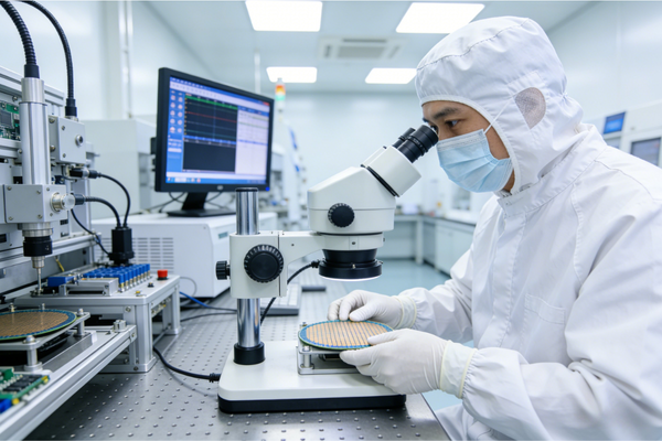
Semiconductor Testing
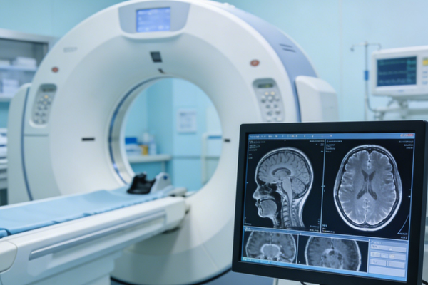
Medical Imaging

Aerospace

Industrial Automation
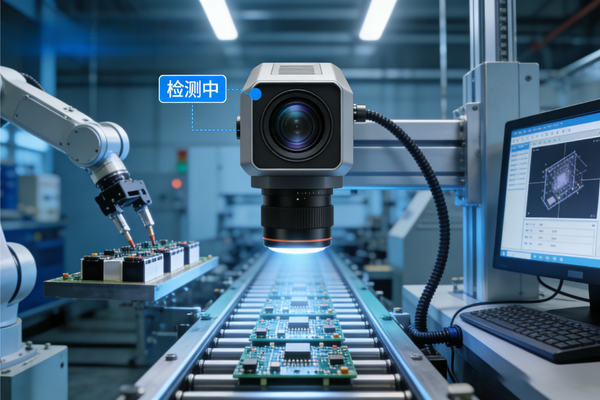
Machine Vision

Precision Testing
