
JetKU‑Based Test for HikRobot MV‑CH040 Camera
JetKU‑Based Test for HikRobot MV‑CH040 Camera
1 Introduction
1.1 Test Overview
This test is carried out based on the JetKU platform developed by Chongqing Star‑Test Electronics. The device under test is the HikRobot MV‑CH040 area‑scan camera. This camera supports Base / Medium / Full / 80‑bit operating modes. The Img‑Grab host‑side software is used for camera parameter configuration and image preview & acquisition. Base, Medium and Full modes support multiple image formats, while the 80‑bit mode only supports the Mono8 image format. Stable operation is achieved for both the acquisition platform and the camera under all four modes. Frame rate can reach over 300 FPS in 80‑bit mode.
1.2 Camera Link Protocol Introduction
Camera Link is a serial communication protocol standard designed for industrial camera interfaces. It standardizes interconnections for scientific and industrial video equipment, including cameras, cables and frame grabbers. Three configurations are defined: Base, Medium and Full, to satisfy different data bandwidth requirements. Camera Link is a mature standard, which transmits video data via LVDS source‑synchronous timing, control data over serial ports, and other trigger & auxiliary signals using four pairs of LVDS I/O lines.
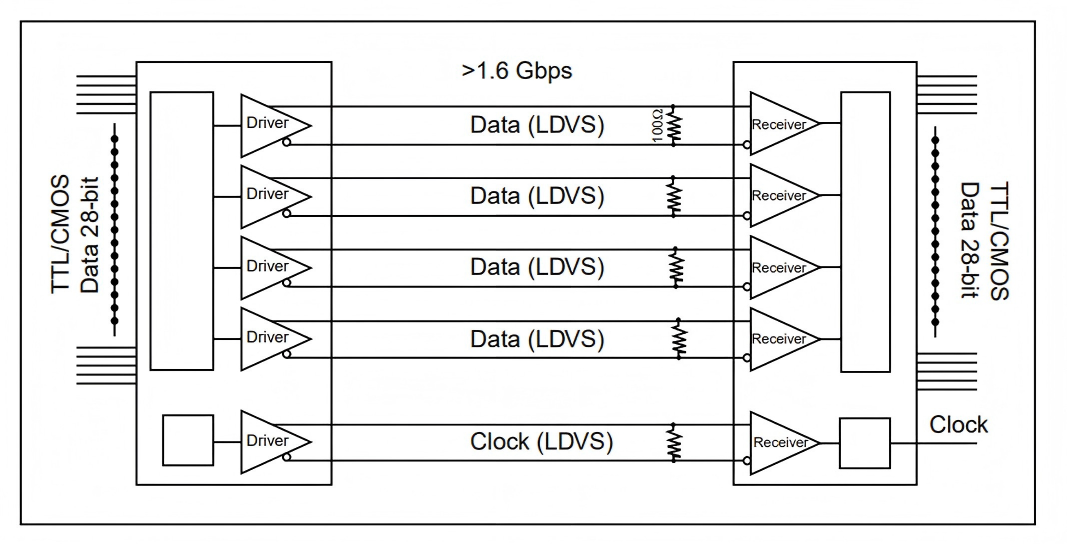
Figure 1‑1 Channel Link Schematic Diagram
Conventional Channel Link implementations rely on dedicated serial‑to‑parallel chips such as DS90CR288 / DS90CR287. These chips consume a large number of I/O resources and require HPC‑type FMC connectors for Full‑mode operation, which limits deployment scenarios. Since Channel Link is essentially serial‑parallel conversion, it can be implemented purely inside FPGA logic. For this reason, we have developed a Camera Link Full input board using native FPGA LVDS interfaces, with expanded multi‑channel FPGA I/Os for user‑defined peripheral connections.
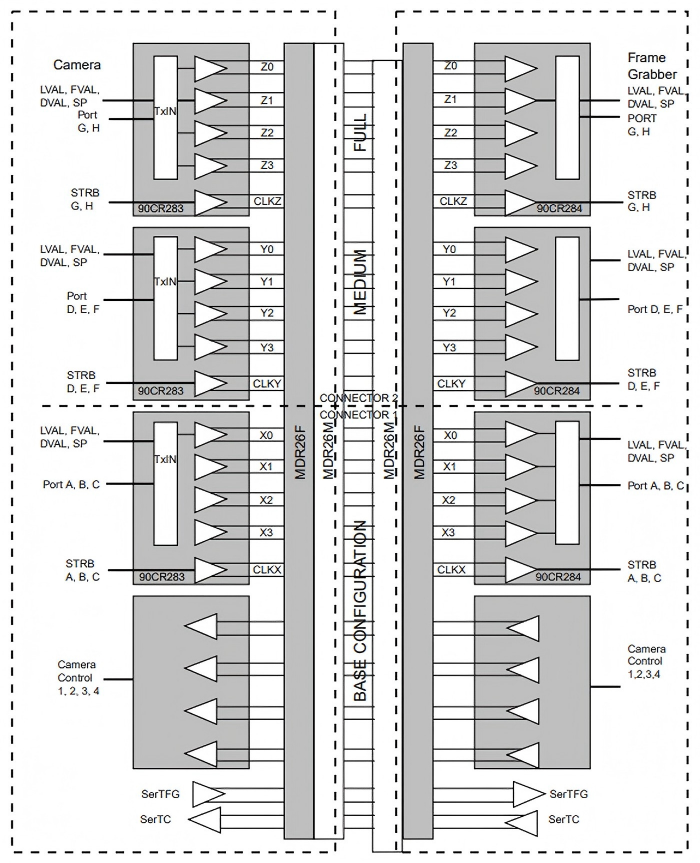
Figure 1‑2 Diagram of Base, Medium and Full Configurations
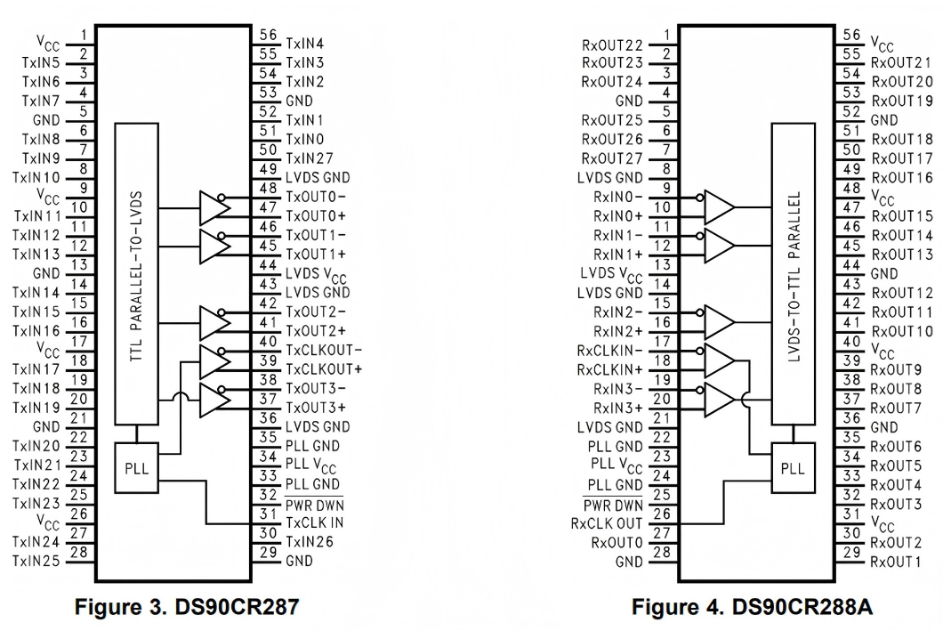
Figure 1‑3 Dedicated Channel Link Serial‑to‑Parallel Converter Chip
The 80‑bit mode has different bit assignments compared with Base / Medium / Full, but shares the same physical hardware requirements as Full mode: three serial‑parallel chips and two cable connectors. Under 80‑bit mode, Ports A‑I are utilized. Original DVAL and spare signals are repurposed as data lines. Only the first Channel‑Link group carries FVAL and LVAL signals; the other two Channel‑Link groups transmit LVAL only. The table below defines bit mapping for 80‑bit, 10‑tap / 8‑bit mode.
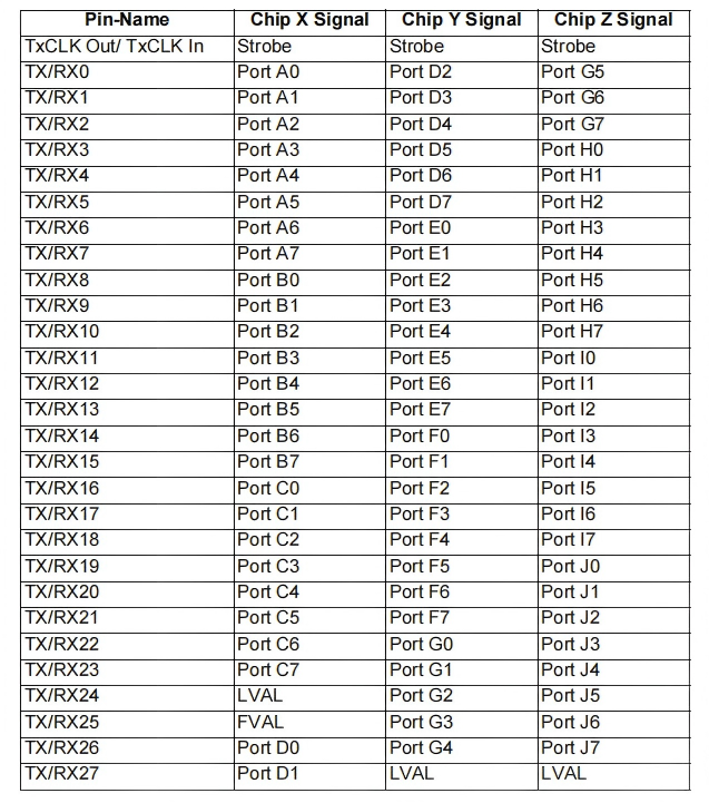
Figure 1‑4 80‑bit Bit Assignment

Figure 1‑5 80‑bit 10‑tap / 8‑bit Mode
2 Hardware Description
2.1 Jetson Overview
NVIDIA Jetson is a family of embedded computing platforms built for edge‑AI and robotics applications. It integrates high‑performance GPU, CPU and dedicated AI accelerators with low‑power profiles, designed for local on‑device AI inference instead of cloud computing. Typical use‑cases include robots, UAVs, smart cameras, industrial automation, medical instruments and autonomous mobile robots.
2.1.1 Key Features
- AI at the Edge: run deep‑learning models locally (object detection, semantic segmentation, speech recognition, etc.) without network dependency.
- Unified software stack: built upon NVIDIA JetPack SDK, including Ubuntu Linux, CUDA, cuDNN, TensorRT, OpenCV and ROS. Software ecosystem is compatible with NVIDIA data‑center GPUs.
- Modular architecture: Jetson modules adopt SoM (System‑on‑Module) plus carrier‑board form‑factor for easy system integration.
- High energy efficiency: delivers tens to hundreds of TOPS AI compute within a 5W‑60W power envelope.
2.1.2 Product Overview
The JetKU‑CameraLink Frame Grabber is a high‑performance embedded image acquisition solution targeting industrial and scientific imaging. Built on the in‑house JetKU platform, the system combines Xilinx Kintex UltraScale+ XCKU5P FPGA and NVIDIA Jetson GPU. Data communication between FPGA and Jetson runs over PCIe Gen3 x4 high‑speed bus. It delivers powerful real‑time pre‑processing and AI inference, together with flexible user‑logic extension capabilities.
For video interfaces, the frame grabber extends Camera Link functions via FMC daughter‑cards. High‑speed image transmission strictly complies with Camera Link LVDS specifications. This hardware focuses purely on image data transfer; cameras must be powered by an independent external power supply.
Benefiting from JetKU computing resources, PCIe Gen3 x4 high bandwidth and on‑board 2GB DDR4 SDRAM buffer, the grabber reliably handles high‑frame‑rate, large‑volume industrial and scientific vision workloads, providing stable low‑latency data capture for edge‑vision systems.
Board Features:
- Xilinx Kintex UltraScale+ XCKU5P‑2FFVB676‑I FPGA
- Supports Camera Link Base / Medium / Full modes via FMC daughter‑card with native LVDS interfaces
- External cameras require separate power supply; Camera Link cables carry only image and control signals
- Rich External I/O including RS‑485, opto‑isolated input / output, LVDS and TTL for complex control scenarios
- NVIDIA Jetson Nano / NX GPU module for power‑efficient edge‑AI workloads
- FPGA‑Jetson interconnection via PCIe Gen3 x4. SDK and demo examples for Camera‑Link cameras are provided for Jetson
- Aravis SDK & GenTL Producer SDK are provided, compatible with most mainstream cameras. SDK and sample code run natively on Jetson for easy edge‑side algorithm deployment.

Figure 2‑1 JetKU‑CameraLink Interface Diagram (Front View)
2.2 MV‑CH040 Camera Overview
The HikRobot MV‑CH040 industrial area‑scan camera transmits uncompressed image data over Camera Link. Parameters and image capture can be configured using Star‑Test’s Img‑Grab software; serial‑port tools support parameter‑only configuration.
Key Specifications:
- High dynamic range and signal‑to‑noise ratio for excellent image quality
- Supports Base / Medium / Full / 80‑bit working modes
- Compliant with Camera Link protocol and GenICam standard
The internal block diagram is shown below. Image data from the sensor goes through on‑board ISP image‑processing pipelines, and is finally transmitted at high speed via the Camera Link physical layer.
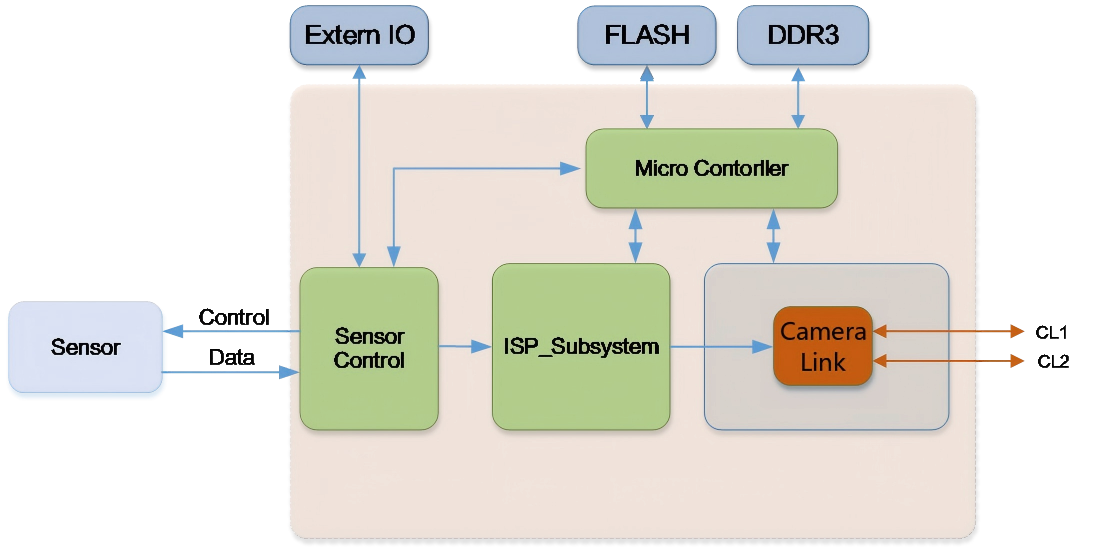
Figure 2‑2 Working Principle
Camera Interface Description:
- CL1: Primary Camera‑Link SDR port for image data and serial‑port communication
- CL2: Secondary Camera‑Link SDR port for image‑data transmission
- Power & I/O connector: supplies power, general‑purpose I/O and serial‑port signals
- Status LED indicator: fast‑blinking blue LED indicates normal image output.
3 Operation Instructions
3.1 Hardware Connection
Power‑on procedure: Connect a 12V DC power supply with a 5.5 mm × 2.1 mm barrel connector to the frame‑grabber power‑in terminal. Supply 12 V DC power to the HikRobot industrial camera. Use Camera‑Link‑certified SDR cables: plug one end into the camera Camera‑Link port and the other end into the corresponding SDR port on the frame‑grabber front panel. For the HikRobot MV‑CH040‑A0CM camera targeting 300 FPS performance, both Camera‑Link ports must be connected: camera CL1 connects to grabber Base port, camera CL2 connects to grabber Full port.
3.2 Camera Configuration
Remote preview and debugging can be performed via host‑PC control mode. Using standard GenTL / Aravis protocols, Jetson acts as a network image server, so an external PC can pull images and adjust camera parameters remotely.
Install drivers and ImgGrab software on your PC (download page: https://img‑grab.com).
1. Ensure your PC and JetKU‑CameraLink unit are on the same local‑area network.
2. Launch ImgGrab; the software will automatically discover JetKU‑CameraLink devices on the network.
3. Click “Connect” to adjust parameters, view real‑time preview and run capture tests.
Note: This host‑side preview mode is intended for debugging or low‑frame‑rate viewing only.
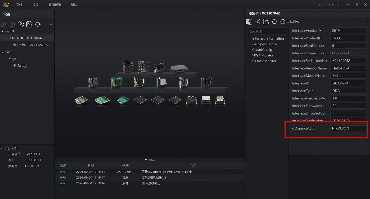
Figure 3‑1 Software Connection Interface
After the device is detected, manually set CLCameraType parameter to HIKVISION. Apply the setting and click the refresh button on the left sidebar to reload device metadata. After successful refresh, the correct device name “HIKROBOT‑MV‑CH040” will appear. Double‑click the device entry or click the connect button to establish communication.
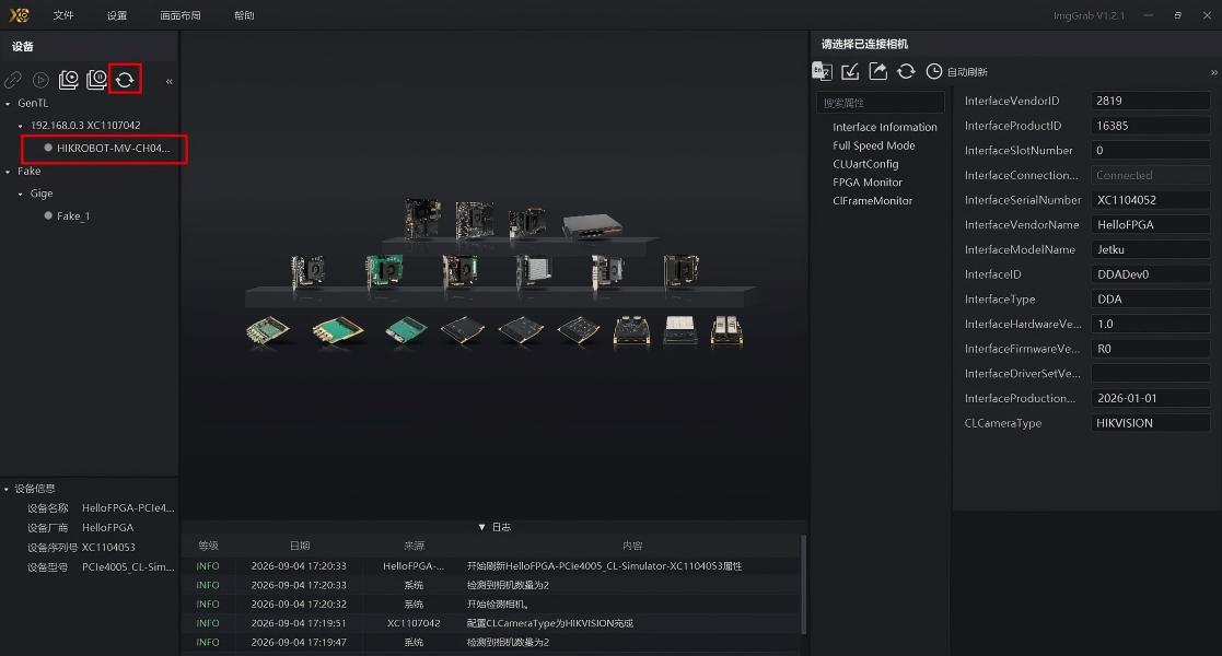
Figure 3‑2 Update Device Information
When connection succeeds, a green status indicator appears beside the device name and the capture workspace opens. Camera parameters can be modified in the right‑hand property panel.
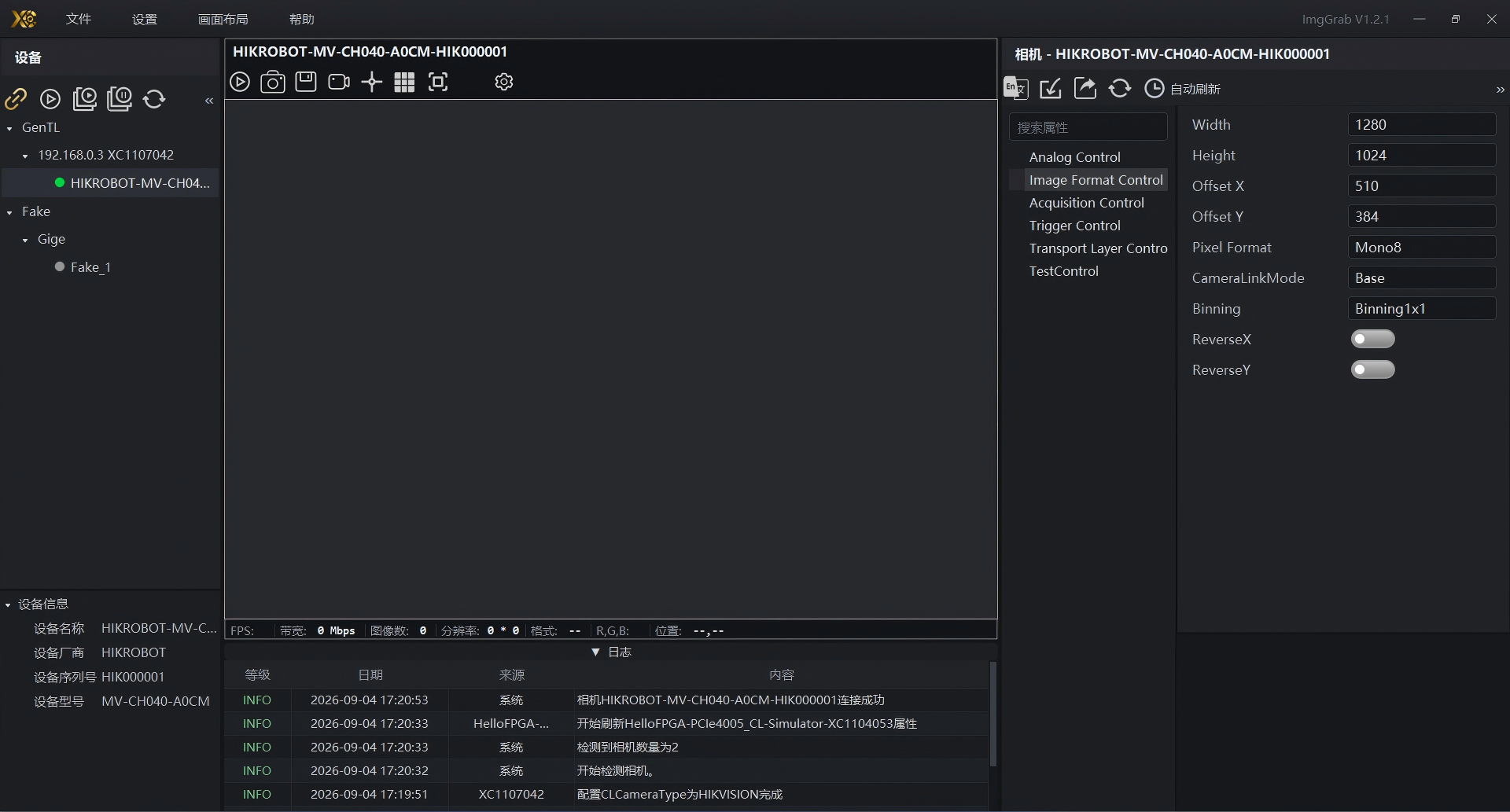
Figure 3‑3 Camera Configuration Interface
Under 80‑bit mode the camera can achieve over 300 frames‑per‑second. Navigate to Image Format Control and set CameraLinkMode to 80‑bit. Set Pixel Format to Mono8. Keep image resolution at 1280 × 1024. Inside Transport Layer Control configure TapCount as Tap10, and keep pixel clock at 85 MHz.
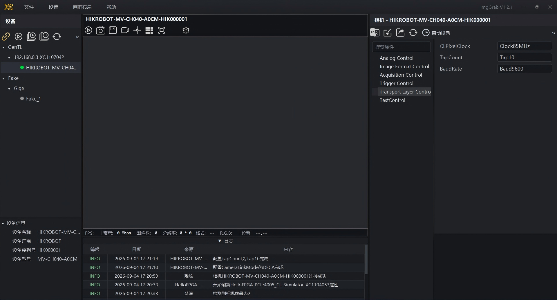
Figure 3‑4 Camera Configuration
Go to Acquisition Control to configure frame‑rate and exposure parameters. In this test case frame‑rate is set to 300 Hz and exposure time is set to 1000 µs.
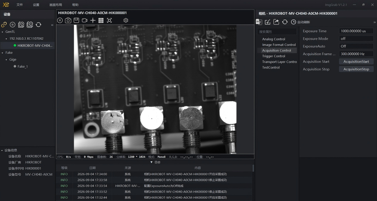
Figure 3‑5 Frame Rate and Exposure Time
Note: 80‑bit mode strictly requires Mono8 pixel format; other pixel formats are unsupported. Image width must use step size of 10 (width value must be divisible by 10). The achievable frame‑rate is affected by image height and exposure duration. If you cannot reach 300 FPS, reduce image height or shorten camera exposure time.
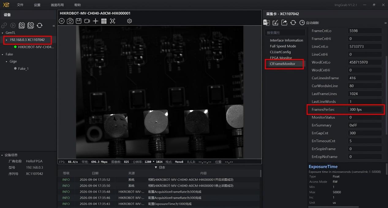
Select the frame‑grabber device in the left‑hand device tree, open CLFrameMonitor under grabber property panel and enable monitoring mode. Real hardware frame‑rate statistics can be read from the FramePerSec field. The FPS value displayed at the bottom of ImgGrab preview window represents network‑transmitted throughput, not the true hardware capture frame‑rate.