

How AI Generates Pin Mapping from PDF Schematics to Simplify FPGA Development
How AI Generates Pin Mapping from PDF Schematics to Simplify FPGA Development
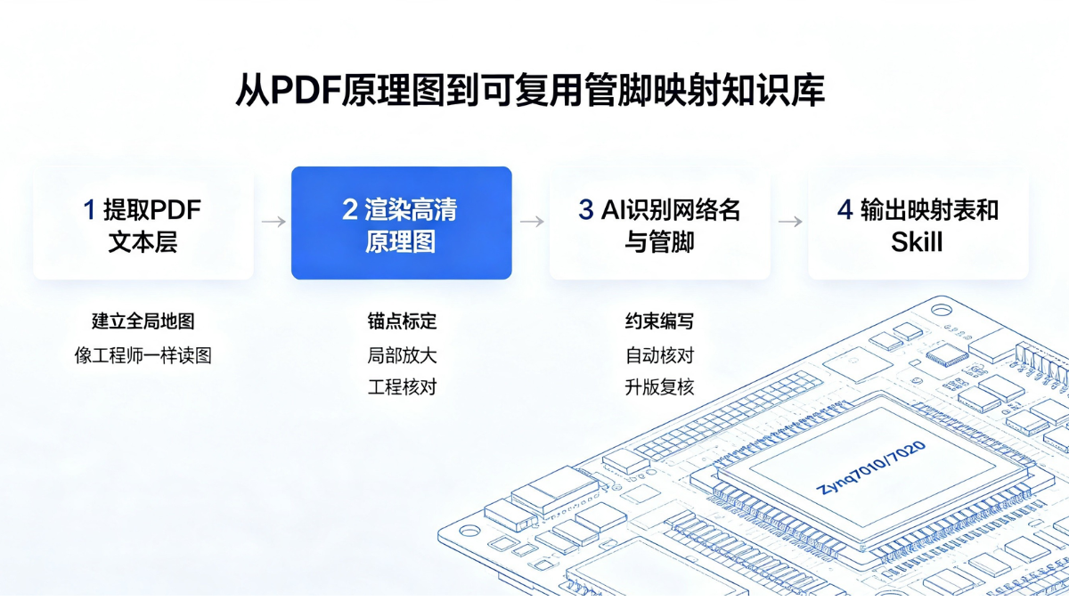
Taking the schematic of a Zynq7010/7020 core board (12 pages, over 400 pin entries) as an example, this paper reviews the complete practice of AI Agent from PDF schematics to reusable pin mapping knowledge base, and how it reshapes the workflow of constraint writing & verification for FPGA. Early attempts yielded poor results, yet current tests prove AI fully capable of this task, bringing us closer to full automation.
Key takeaways:
- Input 1-2 validated reference pin mapping samples;
- Adopt paid LLMs: Alibaba Qwen3.8-Max and Qoder are recommended;
- Export outputs to Skill to avoid repetitive work.
1. Pain Points: Pin Mapping Is the Most Manual Step in FPGA Development
Engineers working on FPGA carrier boards are familiar with this tedious task: after hardware schematics are finalized, thousands of constraints must be written into XDC files:
The core burden lies in manual transcription: converting net name such as B34_L11_P to corresponding package pin U14 requires manual lookup and typing. A full Zynq core board carrier system contains hundreds of pins, including:
- PL domain differential & single-ended IO on Bank34 / Bank35 / Bank13;
- 54 MIO interfaces of the PS domain (QSPI, UART, RGMII, USB, SD, eMMC);
- 70+ address, data and control signals for DDR3;
- 200 pin definitions of two 100-pin board-to-board connectors.
Manual copying has three major drawbacks: time-consuming (half a day to a full day), error-prone (swapped P/N bits, wrong digits cause timing violation or even chip burnout on hardware), and hard to archive. All pin mapping data is scattered in personal Excel sheets; new engineers or schematic revisions require full rework.
2. Challenges: PDF Schematics Are Not Machine-Readable Natively
The intuitive idea of directly parsing PDF files hits multiple roadblocks, as schematics differ greatly from ordinary documents:
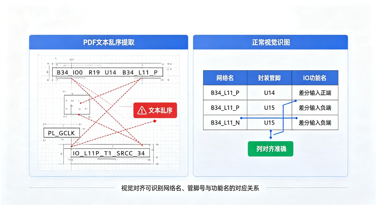
- Text order ≠ visual reading order. Text extracted via pdfplumber becomes disordered fragments:
Texts of FPGA pins on left/right schematic pages interlace randomly, making it impossible to match each pin to its corresponding net name.
- Distorted character rendering. Texts on EDA drawing frames are drawn character by character, leading to overlapping strings like DDDeeesssiiigggnNNNaaammmeee, even misrendering GND5 as 51DNG.
- Data relies on visual alignment. Pairs like B34_L10_P ↔ V15, B34_L10_N ↔ W15 only align horizontally on drawings; minor text offset leads to mismatched pins.
Conclusion: Raw OCR and plain text extraction are unreliable. AI must "view" schematics like human engineers with multi-layer engineering validation.
3. Implementation: Four-Step Automated Pipeline
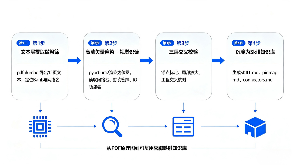
Step 1: Coarse Filter via Text Extraction
Export all text of 12 schematic pages with pdfplumber. The goal is not direct data use, but positioning each Bank and critical net name (B34_L11, Header_2X50) to build a global coordinate map of the design.
Step 2: High-Res Vector Rendering + Visual Recognition
Render each page to 2526×1785 bitmap with pypdfium2 (true vector rendering, not scanned images). The AI vision module reads tables directly and aligns net name, package pin and IO function columns in one pass. Vector-based schematics deliver far higher accuracy than scanned OCR results.
Step 3: Three-Layer Cross Verification
- Anchor Calibration: Feed validated samples (B34_L11_P ↔ U14, B34_L11_N ↔ U15) to train the alignment logic for net/pin columns;
- Local Zoom-In: Zoom suspicious pin regions at 6× resolution to eliminate ambiguous matching;
- Engineering Cross-Check: Compare against warehouse Constraints/*.xdc files. We found legacy XDC pins mismatched this core board (different FPGA package for the carrier board), a risk missed by manual reuse.
Step 4: Archive as Skill Instead of Static Spreadsheets
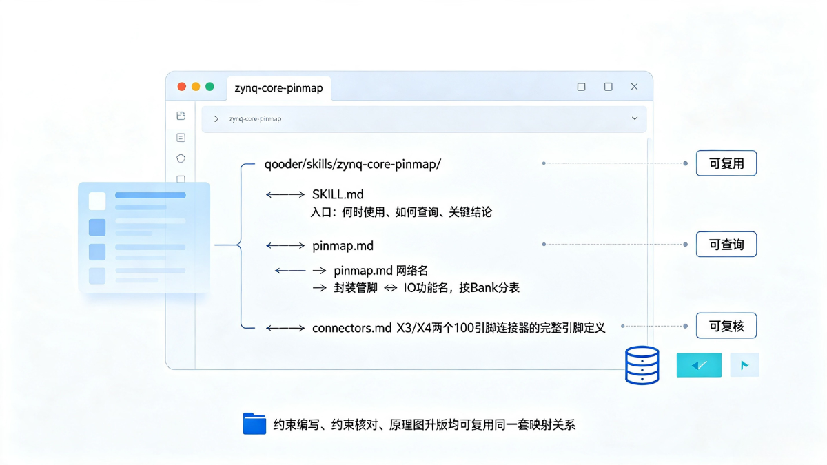
Outputs are stored in a code repository folder instead of Excel:
.qoder/skills/zynq-core-pinmap/
├── SKILL.md       # Guide: Usage, query rules & key conclusions
├── pinmap.md      # Net Name ↔ Package Pin ↔ IO Function, grouped by Bank
└── connectors.md  # Full pin definition for X3/X4 100-pin connectors
This is the core optimization for streamlined FPGA development: the pin mapping dataset becomes reusable AI context, supporting three scenarios:
- Constraint Writing: Input "route AD7606C data lines to Bank34", AI generates correct PACKAGE_PIN definitions;
- Constraint Verification: Auto-scan XDC and flag mismatched pins;
- Schematic Revision: Re-run extract_pdf.py / render_pages.py for fast updated validation.
4. Performance Comparison
| Metric | Manual Transcription | AI Pipeline |
|---|---|---|
| Time Cost | 0.5 ~ 1 workday | Several minutes |
| Coverage | Only frequently used pins | Full Bank + connectors, 400+ entries |
| Error Rate | Dependent on operator care | Anchor + vision + triple engineering validation |
| Data Archive | Personal Excel | Repo Skill, shared by team & AI |
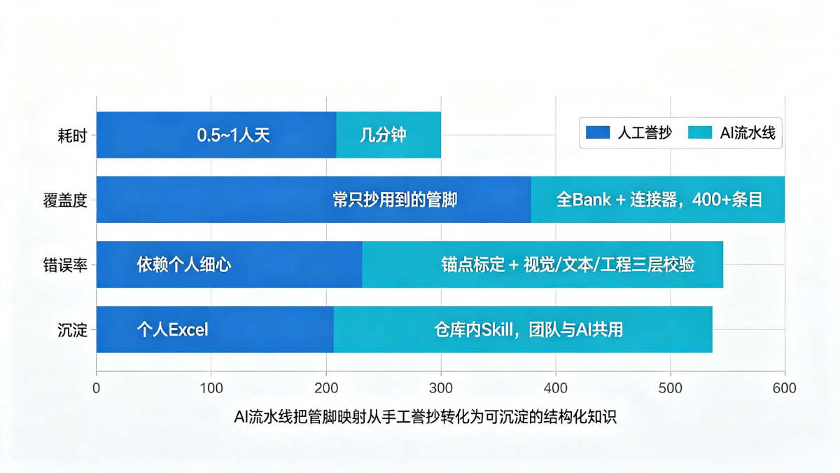
More importantly, cross-verification reveals hidden package pin inconsistency in legacy projects; the value of a unified pin mapping library lies in both generation and continuous design review.
5. Experience & Outlook
- Treat PDF schematics as dual-channel input (image + raw text); single-source parsing is unreliable;
- Calibrate with a small set of anchor pins (one validated pin mapping sample eliminates systemic full-table errors);
- Deliver structured knowledge (Skill / knowledge base) instead of temporary tables, reusable for constraint writing, review and carrier board design;
- The pipeline extends to all "PDF schematic → pin/net list" workflows, including power domains, voltage levels and pull-up/down signal documentation.
When AI converts schematics into machine-readable pin mapping knowledge base, FPGA engineers can focus on core design instead of repetitive manual transcription work.

