
High-Performance 4-Channel CoaXPress Frame Grabber PCIe1004
Hello-FPGA PXIe1004 User Manual
1 Introduction
1.1 CoaXPress Overview
CoaXPress (abbreviated as CXP) refers to a camera data transmission standard using coaxial cables for interconnection, mainly designed to replace the previous Camera Link protocol. It is commonly used in scientific cameras, industrial cameras, medical imaging, aerospace and defense applications. Due to cable type, transmission speed and other factors, Camera Link is no longer suitable for the ever-growing demand for data bandwidth.
CXP is an asymmetric high-speed point-to-point serial transmission protocol, mainly used for transmitting video and still images, with single or multiple coaxial cables typically used. The current 2.0 standard supports a maximum speed of 12.5 Gbps per lane. In addition to transmitting image data, each lane can also carry low-speed control signals (41.6 Mbps) and supply power to the camera via the same cable (Power-over-Coax), with a maximum cable length of 100 meters for a single cable.
The maximum line rate of a single coaxial cable is 12.5 Gbps, and single or multiple cables can be used. For example, four cables can provide a maximum data rate of 50 Gbps.
Long cable lengths are supported: up to 100 meters at 3.125 Gbps, and up to 35 meters at 12.5 Gbps.
Data transmission features real-time performance and low latency, with fixed latency.
Precise real-time triggering capability, supporting trigger transmission via coaxial cable without additional communication cables.
Flexible and reliable performance can be achieved by using standard coaxial cables such as RG59 and RG6 (RG6 is recommended).
Easy integration: images, control communication, and power can be transmitted through a single cable, and cables are cost-effective.
CXP is a point-to-point scalable interface, with 75Ω coaxial cables as the physical medium between devices and HOST. Each CXP interface includes one MASTER connection and several optional extended SLAVE connections, each requiring one coaxial cable. Devices typically number these connections, with MASTER fixed as 0 and SLAVE extended interfaces incrementing sequentially.
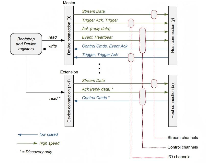
Figure 1-1 CXP Connection Structure
Each connection includes the following functions:
High-speed serial data (typically Device to Host Downconnection), up to 12.5 Gbps.
Low-speed serial data (typically Host to Device Upconnection), up to 41.6 Mbps.
Power supply function (Host to Device), up to 13W.
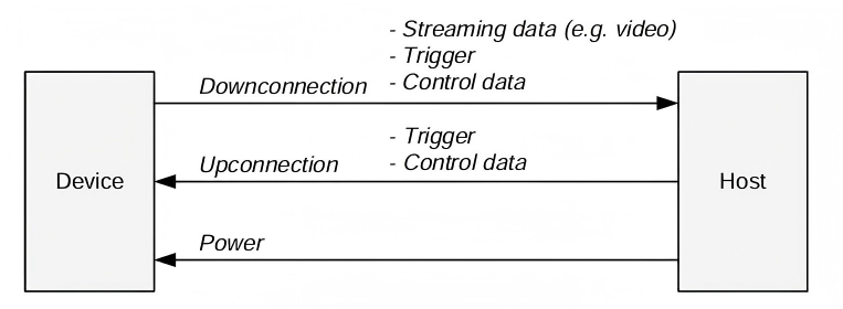
Figure 1-2 DownConnection and Upconnection
Table 1-1 CoaXPress Supported High-Speed Signal Rates
| CXP Speed | Bit Rate (Gbps) |
|---|---|
| CXP-1 | 1.250 |
| CXP-2 | 2.500 |
| CXP-3 | 3.125 |
| CXP-5 | 5.000 |
| CXP-6 | 6.250 |
| CXP-10 | 10.000 |
| CXP-12 | 12.500 |
1.2 Product Overview
HELLO-FPGA PXIe1004 is a high-performance four-channel CoaXPress (CXP) image acquisition card specifically designed for industrial imaging applications. This board supports the latest CoaXPress V2.0 standard, enabling simultaneous transmission of high-speed image data and power (Power over CoaxPress, PoCXP) through a single coaxial cable, simplifying system integration and wiring complexity. In addition, it provides rich external interfaces and internal expansion interfaces to meet various industrial automation requirements.
The PXIe1004 adopts AMD Virtex UltraScale+ FPGA as the core processing unit, providing powerful real-time image preprocessing capabilities and flexible user logic expansion options. It features top-tier logic and DSP resources, delivering strong parallel computing power, and achieves outstanding data throughput through high-speed interfaces such as GTY transceivers and PCIe.
When used with a 4R type daughter card, this board enables CXP interface conversion. Through the CXP interface on the daughter card, it can communicate with external cameras or analog sources, collect data signals from the opposite end into the PXIe1004 board via CXP cables, perform corresponding processing, and then transmit the data to the host computer through the PCIe interface for subsequent processing.
1.3 Key Features
| Category | Feature Description |
|---|---|
| Interface Standard | Supports CoaXPress 2.0, four-channel HDBNC female connectors, each channel up to 12.5 Gbps |
| Host Interface | PCIe Gen3 x8, backward compatible with Gen2/Gen1 |
| FPGA Platform | Xilinx XCKU060-FFVA1156-2-I, supports user-defined logic development |
| On-Board Memory | 4 GB DDR4 SDRAM (64-bit, 2400 MHz) for frame buffering and data preprocessing |
| Chassis Power Supply | Insert into a dedicated PXIe chassis for power supply and function implementation |
| Status Indication | The FPGADONE indicator on the board will light up after the board starts up normally |
2 Safety and Compliance
2.1 Safety Precautions for Use
Do not disassemble the casing without permission.
Do not hot-plug CXP cables; connect the cables first before powering on.
Do not input power exceeding the rated input voltage range.
Avoid storage and transportation in environments with water splashing, rain exposure, direct sunlight, strong electric fields, strong magnetic fields, severe vibration, etc.
2.2 Electrostatic Discharge (ESD) Guidelines
The PXIe1004 uses high-density FPGAs and high-speed interface chips, which are extremely sensitive to electrostatic discharge (ESD). Improper operation may cause permanent damage to the devices.
Pre-operation Preparation:
Operate in a dry environment (relative humidity <60%);
Use an anti-static workbench and anti-static wrist strap, and ensure reliable grounding;
Store the board in an anti-static bag until installation.
Installation Recommendations:
Remove the board from the anti-static bag only when installation is required;
Hold the board by the edges, avoiding contact with the gold fingers, FPGA, HDBNC interfaces, or I/O pins;
If the board is installed but not used for a long time, keep the host powered off and store it in a dry environment.
3 Quick Start Guide
3.1 Essential for Beginners: Before You Start
Hardware Requirements:
Chassis: Dedicated PXIe chassis
Power Supply: Directly insert into the chassis backplane to power the board
Memory: ≥4GB RAM
Hard Disk: ≥10GB available space
Operating System:
Windows 10/11 64-bit (Older versions of Windows are not recommended as abnormal issues may occur)
Linux Ubuntu 18.04/20.04/22.04 64-bit
3.2 Hardware Installation
3.2.1 Board Installation
Turn off the host power and unplug the power cord, discharge static electricity (anti-static wrist strap is recommended).
Open the chassis backplane, select a PXIe physical slot (it is recommended to use the slot close to the CPU for optimal bandwidth). Align the PXIe1004 acquisition card with the slot, insert it firmly vertically until fully seated,
Ensure the board is fully in contact with the interface in the PXIe chassis. Secure the board to the chassis to prevent loosening.
3.2.2 Power Supply Requirements
External Power Supply: 12V 2A power supply (maximum 5A) provided through a four-channel power cable.
Chassis Power Supply: Power is supplied by inserting into the PXIe chassis, no external power supply required.
4 PXIe1004
4.1 Hardware Features
4 independent interfaces, PCIe Gen3 x8 mode
FMC+, used in combination with FMC 4R daughter card
FMC HPC interface
2 sets of DDR4, model MT40A256M16GE-083E
Power supply to cameras via POC, maximum power of 17W per channel
0°-85°C operating temperature (Industrial Grade)
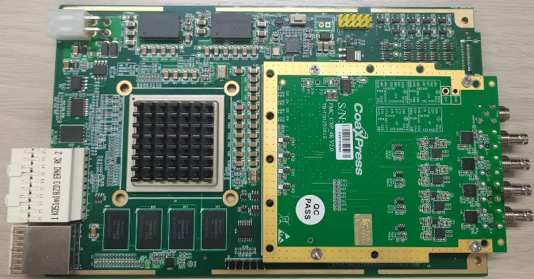
Figure 3-1 Front View of PXIe1004 Board
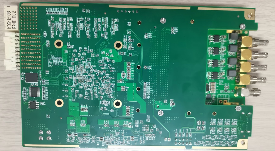
Figure 4-2 Back View of PXIe1004 Board
4.2 Engineering Implementation
4.2.1 Overview of Core Engineering Modules
4.2.1.1 DDR4 IP Core Configuration
The MIG IP controller is a DDR control IP provided by Xilinx for users, enabling users to easily read and write DDR memory through the DDR controller without understanding DDR control and read/write timing.
The DDR controller consists of three parts: User Interface Block, Memory Controller, and Physical Layer of DDR. Developers only need to develop user logic design to interface with the user interface of the DDR controller for reading and writing DDR data. For more information about the interface definition and timing of the DDR controller user side, please refer to the documentation provided by Xilinx (PG150). Next, we will introduce how to generate and configure the DDR controller.
Create a project, open the IP Catalog, and select DDR4 SDRAM (MIG). In the Basic interface, select the system clock corresponding to the board (100MHz) as the reference clock. Select the similar DDR model MT40A256M16GE-083E here, and set Data Width to 64 bits.
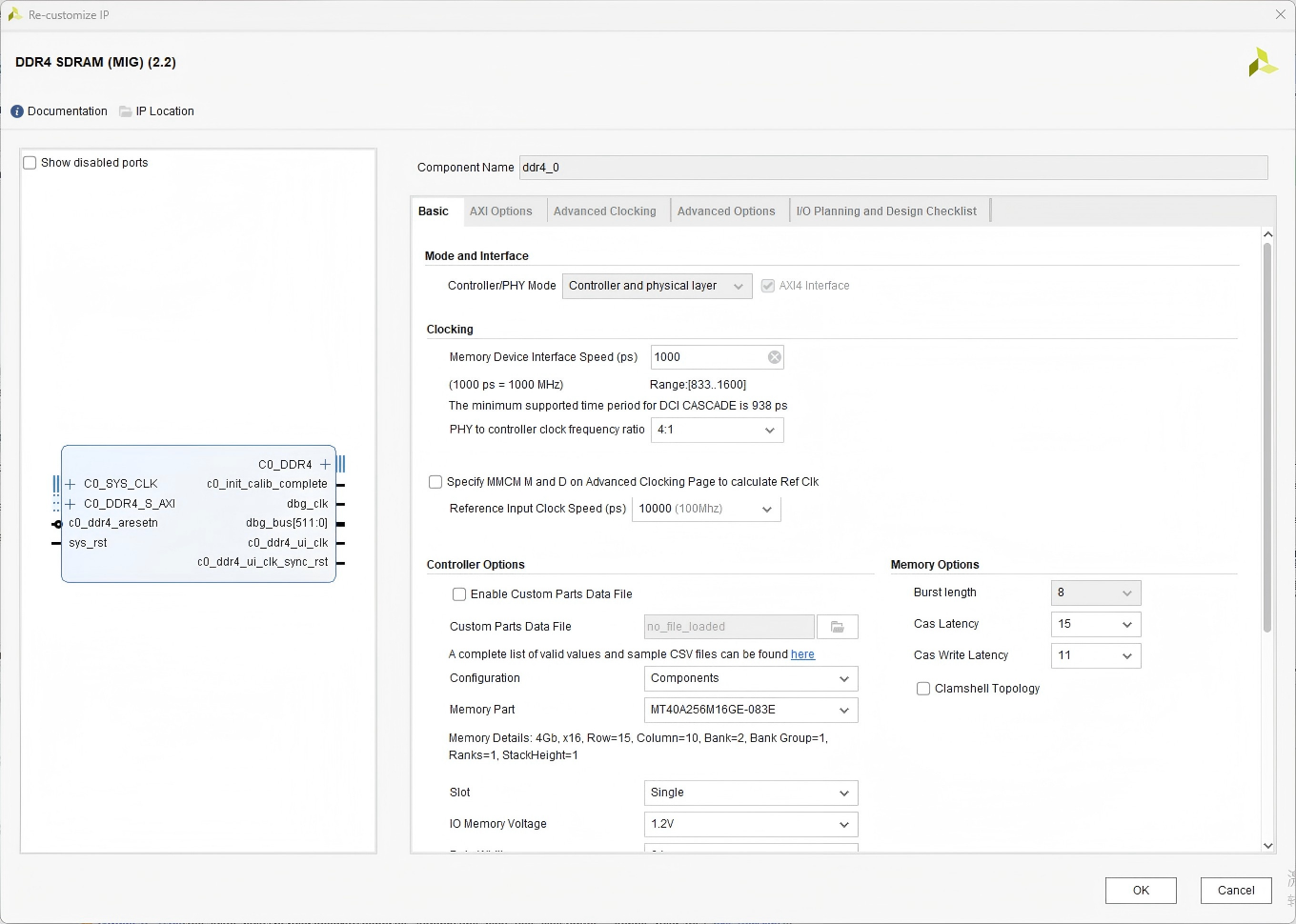
DDR4 MIG Configuration Interface
4.2.1.2 XDMA IP Core
The XDMA IP core (DMA for PCI Express) is a hardware IP core provided by AMD (formerly Xilinx), whose full name is "DMA Subsystem for PCI Express". It is an engine specifically responsible for high-speed data transfer between FPGA and host (CPU memory). It allows you to achieve ultra-high-speed, low-latency data transmission between FPGA and host software through the standard PCIe interface using DMA (Direct Memory Access) technology, with minimal CPU intervention.
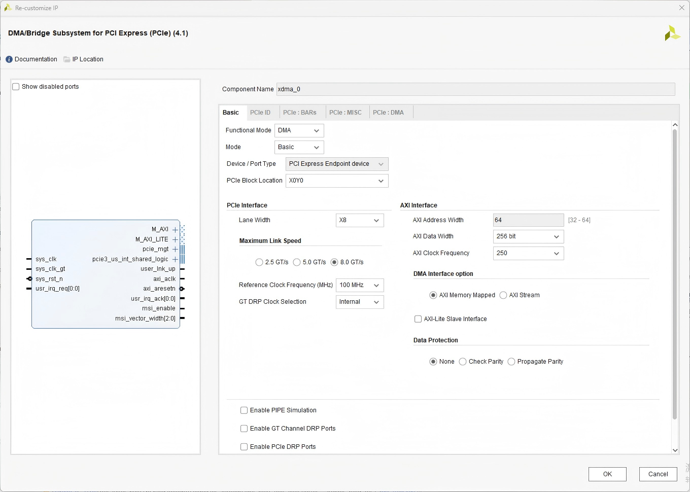
XDMA Module Diagram
In the current project, we use GEN3 X8 mode, so select 8gt/s rate and x8 lane width in the corresponding configuration of the IP.
4.2.1.3 DMA Stream Interface
In the current project, the DMA bit width is 256 bits.
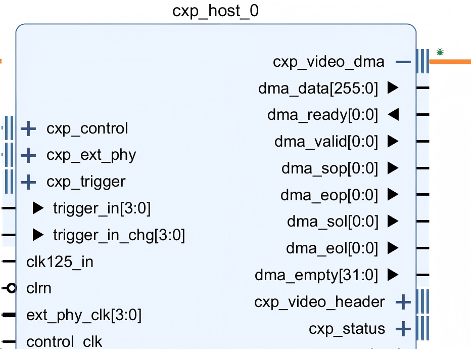
DMA Stream Interface Diagram
Table 4-1 Video Stream DMA Interface
| Signal Name | Input/Output | Bit Width | Description |
|---|---|---|---|
| dma_clk | Input | STREAMS | DMA stream clock. |
| dma_data | Output | 32*STREAM_WORDSxSTREAMS | DMA stream data. |
| dma_empty | Output | WIDTH_O(1)xSTREAMS | DMA empty indication, indicating the last transfer of a frame. |
| dma_valid | Output | STREAMS | DMA stream data valid signal; when this signal goes low, transmission pauses. |
| dma_ready | Input | STREAMS | DMA stream data reception ready signal. |
| dma_sop | Output | STREAMS | Start of frame indication. |
| dma_eop | Output | STREAMS | End of frame indication. |
| dma_sol | Output | STREAMS | Start of line indication. |
| dma_eol | Output | STREAMS | End of line indication. |
Video DMA Stream is a general video stream interface. How do specific data correspond to pixels?
When STREAMS is 1 and STREAM_WORDS is 4, the dma_data bit width is 128 bits, and the data arrangement is as follows:
If the Device transmits 8-bit pixels, the output stream data through the DMA bus will contain 8-bit pixel data, with a total of 16 pixels per clock cycle. Pixel 0 occupies [7:0] of dma_data, pixel 1 occupies [15:8] of dma_data, and so on.
If the Device transmits 10/12/14/16-bit pixel images, the decoded stream will consist of 16-bit pixel data, with a total of 8 pixels per clock cycle. The data is placed in the lower 10/12/14/16 bits of 16 bits. For example, when 12-bit pixel input is used, the 0th pixel is in dma_data[11:0], the 1st pixel is in dma_data[27:16], and so on.
DMA_SOP and DMA_EOP indicate the start and end of a frame, respectively.
DMA_SOL and DMA_EOL indicate the start and end of a line, respectively.
DMA_EMPTY indicates the number of empty bytes in the last transfer frame. In our design, its value is always 0 when data is valid, and the data will be spliced internally.

Figure 4-3 Video DMA Timing
4.2.2 Firmware Programming
Here, the constraint used in our project is SPI×4 mode. SPI×4 only requires a bin file or mcs file generated by the project for programming.
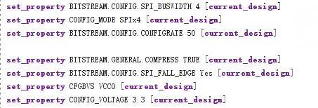
SPIx4 Configuration Code
There are two ways to generate a bin file. First, the official generation method: click Settings in the Tools menu,
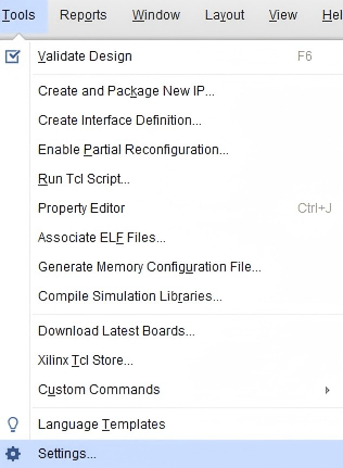
Tools Menu
Enter the settings page, check the bin_file option in the Bitstream page, and the bin file will be automatically generated after compilation is completed. If the project has been compiled but this option was not checked before compilation, you can also check it after compilation and click the generate bitstream option in the GUI. At this time, the project will not be recompiled from scratch, but only regenerate the bit and bin files.
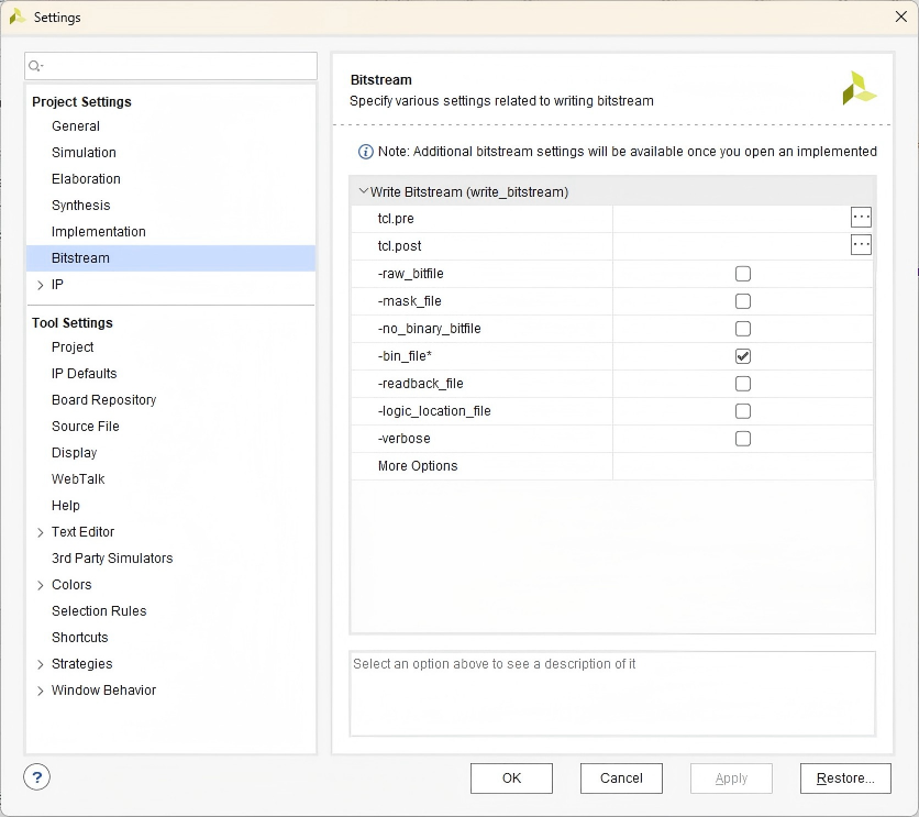
Bitstream Settings
The second generation method is simpler: you can directly modify the suffix of the generated bit file to bin and then program it directly. This is because in principle, the bit file only has an additional header compared to the bin file, and the FPGA can automatically ignore it, so it can be used normally. However, it should be noted that this is only applicable when programming with a single bin file; it will fail if using multiboot startup.
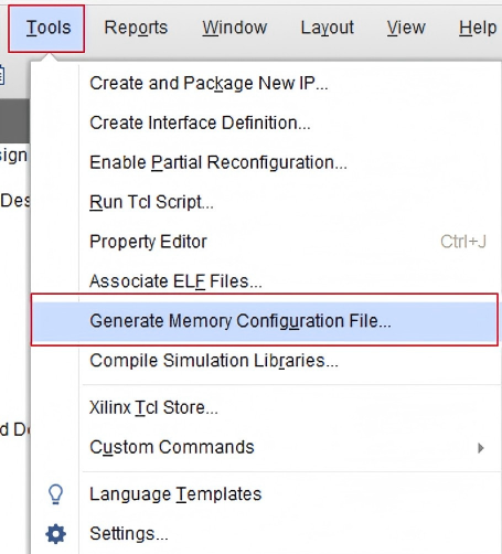
The MCS file is generated by first clicking Generate Memory Configuration File... in the Tools menu.
MCS Generation Interface
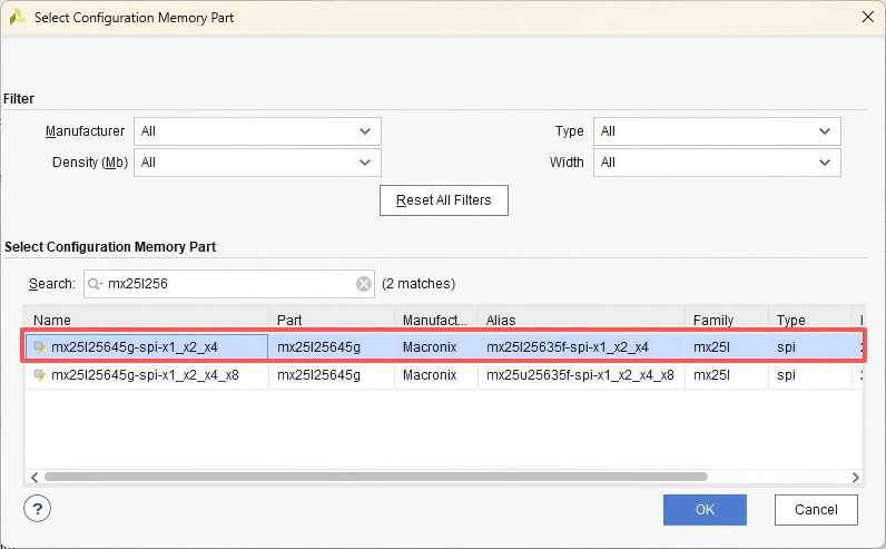
Select MCS as the generated file type, and select the model in the red box in the following figure as the flash model.
Flash Model Selection
Select SPI×4 for the interface, select the bit file generated just now for the bit file, and click OK. Wait for the interface shown in the following figure, indicating that the mcs file generation is completed.
Then program the mcs file according to the previous steps, select the flash model, and select the mcs file we just generated. Click OK. Wait for the file programming to complete.
After programming is completed, when the following window pops up, it can be judged that programming is successful. At this time, power off the board first, then unplug the programmer,
Power on again, and the program in the flash will start after power-on.
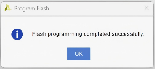
Programming Success Prompt
4.3 ImaGrab
ImaGrab is a Windows/Linux graphical client designed by Xingce Electronics, which can complete CoaXPress device discovery, parameter configuration, real-time preview and image acquisition without programming. It is suitable for on-site debugging, system integration and teaching demonstrations. For more detailed instructions on using the Img-Grab software, please refer to "Img-Grab Application User Manual" https://img-grab.com/filedownload/3000793
4.3.1 Main Functions
- Scan and enumerate all connected PCIe acquisition cards and cameras mounted on the acquisition cards;
- Supports GenICam standard parameter tree (exposure time, gain, trigger mode, ROI, etc.);
- Real-time image display (supports zooming);
- Manual/automatic acquisition control;
- PoCXP power supply switch and current monitoring;
- External I/O trigger signal configuration (input/output direction, level, routing);
- Log export and firmware upgrade entry.
4.3.2 Interface Layout
The ImaGrab client adopts a modular design, and the main interface is divided into six functional areas for efficient user operation and monitoring.

Figure 4-4 ImaGrab Client Main Interface
4.3.3 ImgGrab Quick Usage Process
Start the Software
Double-click the desktop shortcut ImaGrab.exe to launch the client.
Scan and Connect to Camera
Click the [Refresh Devices] button in the toolbar, and the system will automatically scan the acquisition cards in the PCIe slots and the cameras mounted on them; double-click the target camera in the device list (Area 2), and the software will automatically establish a connection, load the GenICam XML description file, and display all configurable parameters in the property tree (Area 5).
Configure Camera Parameters
Width / Height: Set ROI;
ExposureTime: Adjust exposure time;
TriggerMode: Select trigger mode (Off/On);
LineSelector + LineMode: Configure External I/O functions.
Start Image Acquisition
Click the [Continuous Acquisition] button in the toolbar to start the real-time image stream;
Images will be displayed in the preview window (Area 4), along with information such as frame rate and resolution.
Save Images or Videos
Single frame: Click [Save Image], supports BMP/JPG/PNG;
Video: Click [Record Video], saved as .bin format.
4.3.4 GUI Test Examples
4.3.4.1 Imggrab Example
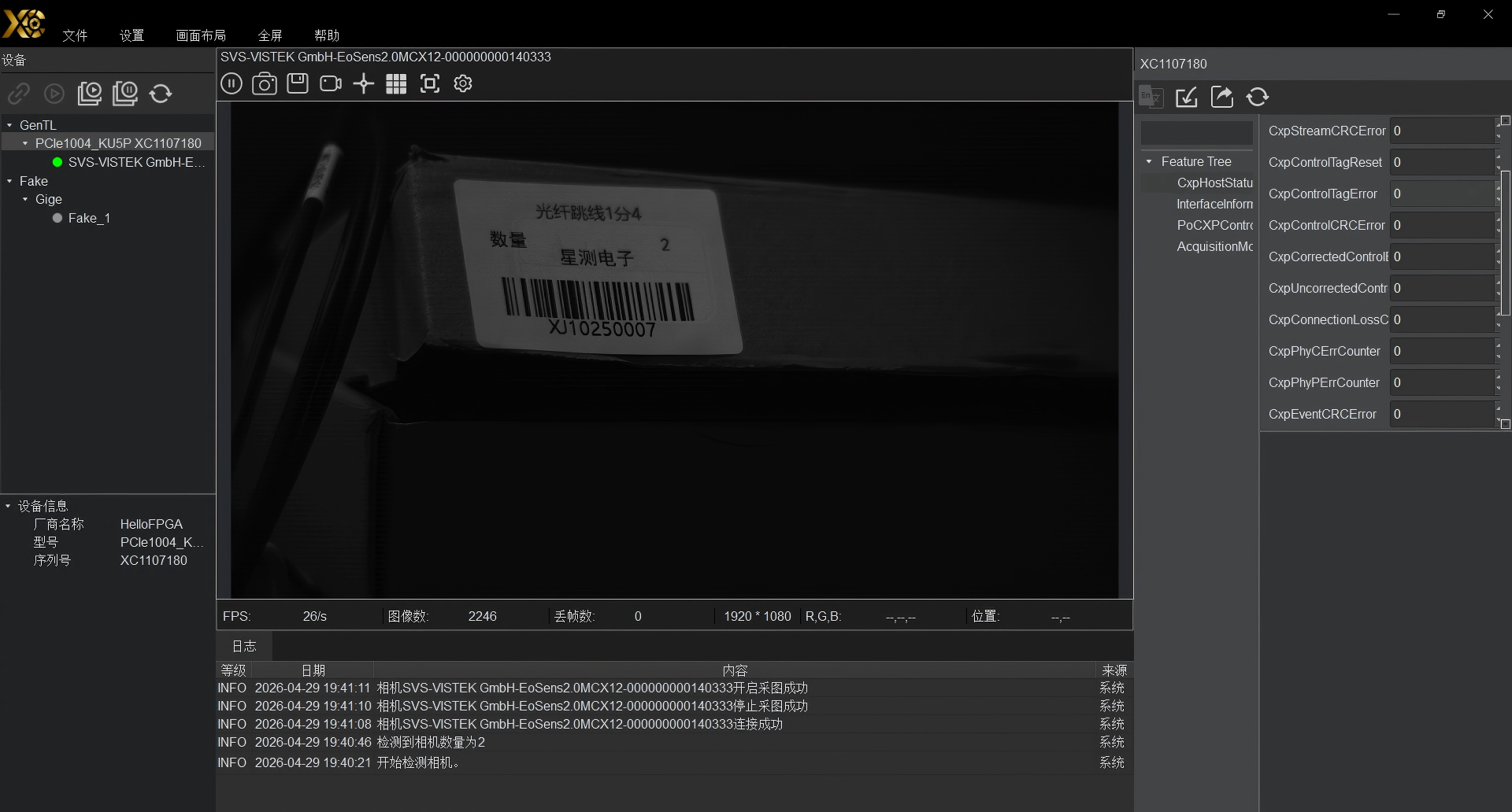
Figure 4-5 ImaGrab Actual Test Image 1
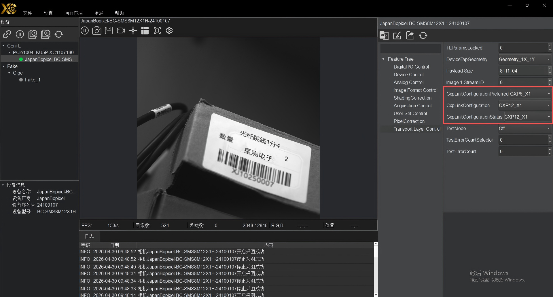
Figure 4-6 ImaGrab Actual Test Image 2
4.3.4.2 Qt Example
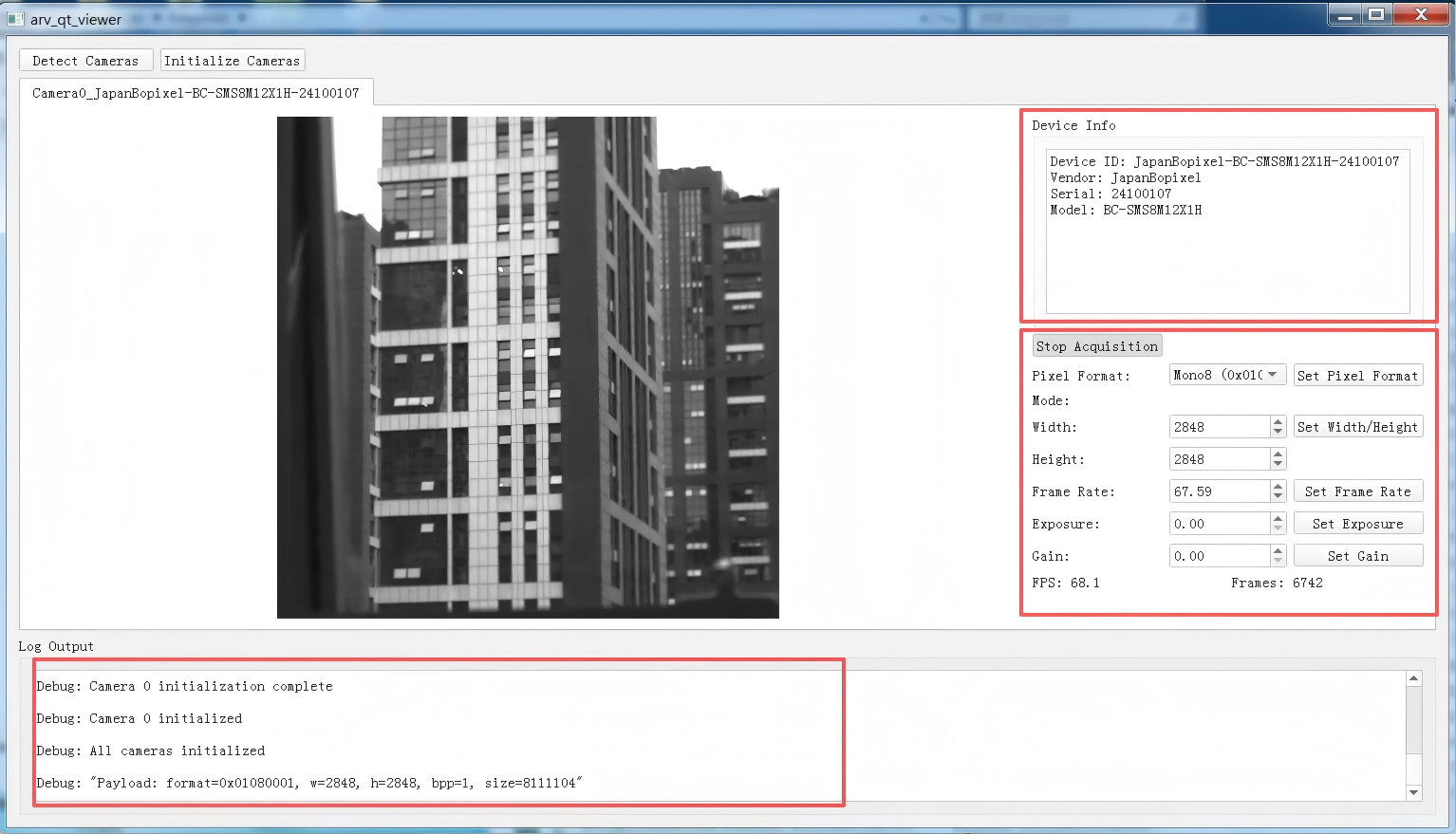
Figure 4-7 QT Example GUI
4.3.4.3 GenTL SDK Test Example
// 1. Initialize GenTL library
GCInitLib();

// 2. Open TransportLayer
TLOpen(&hTL);

// 3. Update Interface list and open the first Interface
TLUpdateInterfaceList(hTL,&changed,2000);
TLGetInterfaceID(hTL,0,ifaceID,&idSize);
TLOpenInterface(hTL,&hIF);

// 4. Update Device list and open the first Device
IFUpdateDeviceList(hIF,&changed,2000);
IFGetDeviceID(hIF,0,devID,&idSize);
IFOpenDevice(hIF,devID,DEVICE_ACCESS_CONTROL,&hDev);

// 5. Get Device Port handle (for reading/writing camera registers)
DevGetPort(hDev,&hDevice);

// 6. Open DataStream
DevGetDataStreamID(hDev,0,dsID,&idSize);
DevOpenDataStream(hDev,&hDS);

// 7. Allocate buffer and register event
DSAnnounceBuffer(hDS,buffer, payloadSize,NULL, &hBuf);
GCRegisterEvent(hDS,EVENT_NEW_BUFFER,&eventHand);
DSFlushQueue(hDS,ACQ_QUEUE_ALL_TO_INPUT);

// 8. Start acquisition
DSStartAcquisition(hDS,0, GENTL_INFINITE);

// 9. Write camera AcquisitionStart register (big-endian conversion)
startReg=swap_uint32(CAMERA_XML_ACQUISITION_START_VALUE);
GCWritePort(hDevice,CAMERA_XML_ACQUISITION_START_REG,&startReg,®Size);

// 10. Poll to get images
EventGetData(eventHand,buffer,&bufferSize,GENTL_INFINITE);
bufferHandle= ((EVENT_NEW_BUFFER_DATA*)buffer)->BufferHandle;
DSGetBufferInfo(hDS,bufferHandle,BUFFER_INFO_BASE,NULL,&imageData,&infoSize);
fwrite(imageData,1, payloadSize,videoFile);
DSQueueBuffer(hDS,bufferHandle);

// 11. Stop acquisition
GCWritePort(hDevice,CAMERA_XML_ACQUISITION_STOP_REG,&stopReg,®Size);
DSStopAcquisition(hDS,0);

// 12. Release resources (strictly in reverse order)
GCUnregisterEvent(hDS,EVENT_NEW_BUFFER);
DSFlushQueue(hDS,ACQ_QUEUE_ALL_DISCARD);
DSRevokeBuffer(hDS,hBuf,NULL,NULL);
DSClose(hDS);
DevClose(hDev);
IFClose(hIF);
TLClose(hTL);
GCCloseLib();
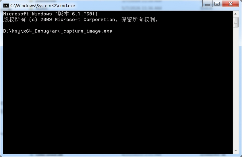
Figure 4-8 Running GenTL SDK Example
For GenTL SDK example testing, we can open a cmd terminal in the folder of the arv_capture_image.exe application, enter commands to run the application, which will start running and identify the device, print out relevant device information, then perform acquisition and save the acquired files.
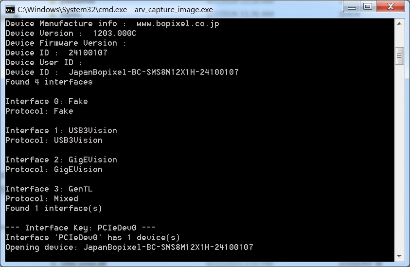
Figure 4-9 GenTL SDK Example Identifying Device Information
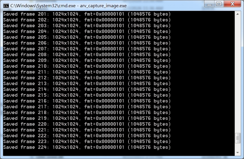
Figure 4-10 GenTL SDK Example Acquisition
The figure below shows each frame of image we acquired and saved, including printed image information.
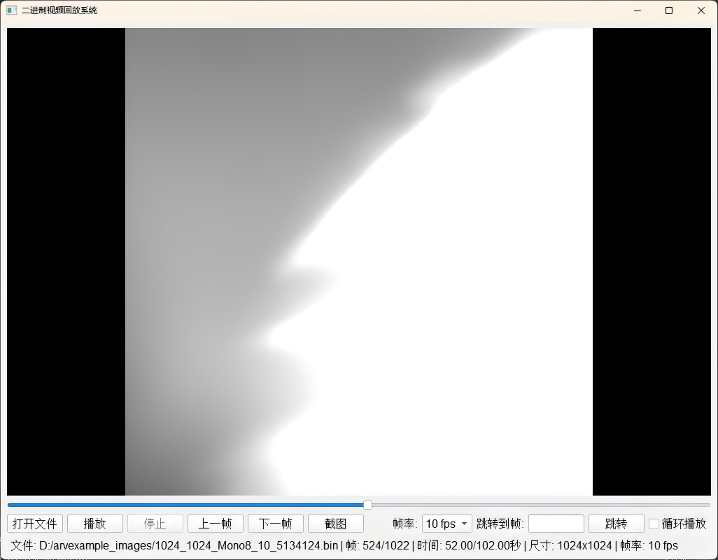
Figure 4-11 Acquired Image Playback GUI
Then we import the saved data into the imggrab host computer for playback to view the acquired image information.
Annex A: Reference Materials
1. CoaXPess JIIA CXP-001-2021
