
Hello-FPGA VU13P_PCIE16 User Manual | 4-Channel CoaXPress 2.0 Image Acquisition Card
Hello-FPGA VU13P_PCIE16 User Manual
1 Introduction
1.1 Introduction to CoaXPress
CoaXPress (CXP) is a camera data transmission standard using coaxial cable interconnection, mainly used to replace the previous Camera Link protocol. It is commonly used in scientific cameras, industrial cameras, medical imaging, aerospace and defense applications. Due to cable form and transmission speed limitations, Camera Link no longer meets the growing demand for data bandwidth.
CXP is an asymmetric high-speed point-to-point serial transmission protocol mainly used for video and still image transmission, typically using single or multiple coaxial cables. The current 2.0 standard supports a maximum speed of 12.5Gbps per lane. In addition to image data, each lane can transmit low-speed control signals (41.6Mbps) and can also supply power to the camera via the cable, known as “Power-over-Coax”. A single cable can reach up to 100m in length.
- Single coaxial cable supports up to 12.5Gbps line rate. Single or multiple cables can be used; for example, 4 cables can provide up to 50Gbps data rate.
- Long cable length: up to 100m at 3.125Gbps, up to 35m at 12.5Gbps.
- Real-time, low-latency data transmission with fixed latency.
- Precise real-time triggering, supports trigger transmission via coaxial cable without additional communication cables.
- Flexible and reliable performance using standard coaxial cables such as RG59 and RG6; RG6 is recommended.
- Easy integration: image, control communication, and power can share the same cable, with low-cost cables.
CXP is a point-to-point scalable interface. The physical medium between device and host is 75Ω coaxial cable. Each CXP interface includes one MASTER connection and several optional extended SLAVE connections. Each connection requires one coaxial cable. The MASTER is fixed as 0, and SLAVE expansion interfaces are numbered sequentially.

Figure 1-1 CXP Connection Structure
Each connection provides the following functions:
- High-speed serial data (typically Device to Host Downconnection), up to 12.5 Gbps.
- Low-speed serial data (typically Host to Device Upconnection), up to 41.6 Mbps.
- Power supply (Host to Device), up to 13W.
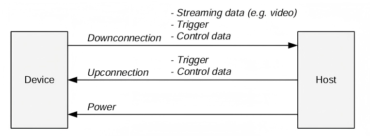
Figure 1-2 DownConnection & Upconnection
Table 1-1 CoaXPress Supported High-Speed Signal Rates
| CXP Speed | Bit Rate (Gbps) |
|---|---|
| CXP-1 | 1.250 |
| CXP-2 | 2.500 |
| CXP-3 | 3.125 |
| CXP-5 | 5.000 |
| CXP-6 | 6.250 |
| CXP-10 | 10.000 |
| CXP-12 | 12.500 |
1.2 Product Overview
HELLO-FPGA VU13P_PCIE16 is a high-performance 4-channel CoaXPress (CXP) image acquisition card designed for industrial imaging applications. The board supports the latest CoaXPress V2.0 standard and can transmit high-speed image data and power (Power over CoaXPress, PoCXP) simultaneously over a single coaxial cable, simplifying system integration and wiring complexity. It also provides rich external and internal expansion interfaces to meet diverse industrial automation requirements.
VU13P_PCIE16 uses AMD Virtex UltraScale+ FPGA as the core processing unit, providing powerful real-time image preprocessing capabilities and flexible user logic expansion options. With top-level logic and DSP resources, it delivers powerful parallel computing power and excellent data throughput through GTY transceivers, PCIe and other high-speed interfaces.
With a 4R-type daughter card, the board can implement CXP interface conversion. Through the CXP interfaces on the daughter card, it communicates with external cameras or analog sources, captures data from the peer device via CXP cables, processes the data inside the VU13P board, and then transmits it to the host computer through the PCIe interface for subsequent processing.
1.3 Key Features
| Category | Description |
|---|---|
| Interface Standard | Supports CoaXPress 2.0, 4-channel HDBNC female connector, up to 12.5Gbps per channel |
| Host Interface | PCIe Gen3 x16, backward compatible with Gen2/Gen1 |
| FPGA Platform | Xilinx XCVU13P-FHGB2104-2-I, supports user-defined logic development |
| On-board Memory | 4 GB DDR4 SDRAM (64-bit, 2400 MHz) for frame buffer and data preprocessing |
| PoCXP Power | 12VDC input via 6-pin PEG socket, up to 24V/1.7A output, with current monitoring |
| Status Indicator | FPGADONE LED lights up when the board boots normally |
2 Safety & Compliance
Please read this chapter carefully before installing, operating or maintaining the CoaXPress Over Fiber Range Extender module. Following these safety guidelines can effectively prevent personal injury, equipment damage or system failure.
2.1 Safety Precautions
- Do not disassemble the enclosure without permission.
- Do not hot-plug CXP cables; connect cables before powering on.
- PoCXP power limit: if using PoCXP to power the camera, ensure sufficient power supply, minimum 12V 3A, recommended 12V 5A/6A.
- Do not input voltage exceeding the rated range.
- Avoid storage and transportation in locations with water splashing, direct sunlight, strong electric fields, strong magnetic fields or strong vibration.
2.2 ESD Guidelines
VU13P_PCIE16 uses high-density FPGA and high-speed interface chips, which are extremely sensitive to electrostatic discharge (ESD). Improper operation may cause permanent device failure.
Preparation Before Operation
- Operate in a dry environment (relative humidity <60%);
- Use ESD workbench and wrist strap, ensure reliable grounding;
- Store the board in an anti-static bag until installation.
- Installation Recommendations
- Remove the board only when ready for installation;
- Hold the board by the edges; avoid touching gold fingers, FPGA, HDBNC interfaces or I/O pins;
- If the board is installed but unused for a long time, keep the host powered off and stored in a dry environment.
3 Quick Start Guide
Welcome to the VU13P_PCIE16 image acquisition card! This chapter helps you complete equipment installation and software configuration quickly from scratch.
3.1 For First-time Users: Before You Start
Hardware Requirements:
- Motherboard: PCIe x8 or x16 slot (PCIe 3.0 or above recommended)
- Power Supply: Rated ≥500W (when using PoCXP, do NOT use ATX 6-pin auxiliary power; power via PCIe only)
- Memory: ≥4GB RAM
- Hard Disk: ≥10GB free space
- Operating System:
- Windows 10/11 64-bit
- Linux Ubuntu 18.04/20.04/22.04 64-bit
3.2 Hardware Installation
3.2.1 Board Installation
Turn off the host and unplug the power cord; discharge static electricity (ESD wristband recommended).
Open the chassis side panel, select a PCIe x8 or x16 physical slot (close to the CPU for best bandwidth). Align the VU13P_PCIE16 card with the slot and insert firmly and vertically until fully seated.
Ensure gold fingers are fully engaged. Secure the rear baffle to the chassis with screws to prevent loosening.
3.2.2 Power Requirements
- Board Power: Powered via PCIe slot (75W standard), no external power required.
- Camera Power: Designed to supply PoC power directly to the camera through the PCIe interface, no external power required.
- Note: The on-board ATX power connector is NOT available.
4 VU13P_PCIE16
4.1 Hardware Features
- 4 independent interfaces, PCIe Gen3 x16 mode
- FMC+ compatible, works with FMC 4R daughter card
- FMC HPC interface
- 2×DDR4, model MT40A512M16HA-083E
- 1×Gigabit Ethernet port
- PoC power supply for cameras, max 17W per channel
- Operating temperature: 0°C to 85°C (Industrial Grade)
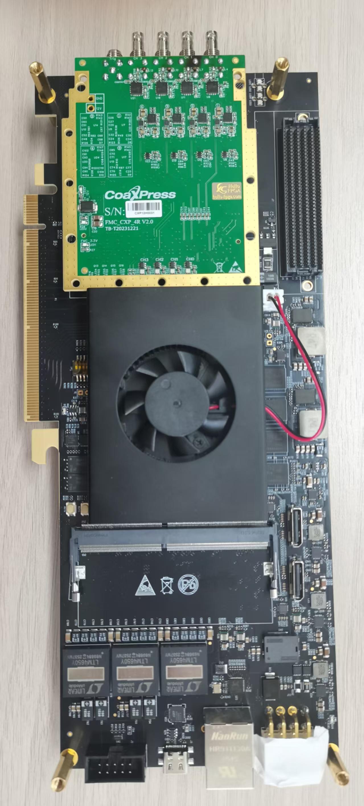
Figure 3-1 VU13P_PCIE16 Board Front View
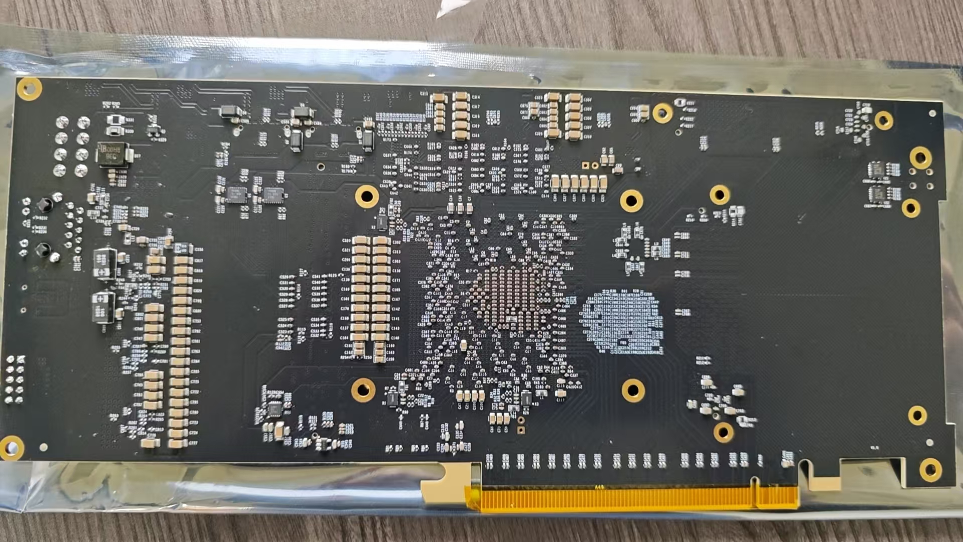
Figure 4-2 VU13P_PCIE16 Board Back View
4.2 Project Implementation
4.2.1 Core Module Introduction
4.2.1.1 DDR4 IP Core Configuration
MIG IP controller is a DDR control IP provided by Xilinx, allowing users to easily read and write DDR memory without understanding DDR control and timing.
DDR controller includes three parts: User Interface Block, Memory Controller and Physical Layer. Users only need to connect user logic to the user interface of the DDR controller. For more details on interface definition and timing, refer to Xilinx documentation (PG150).
Create a project, open IP Catalog, select DDR4 SDRAM (MIG). In Basic page, set reference clock to 200MHz. Select DDR model MT40A512M16HA-083E, Data Width 64-bit.
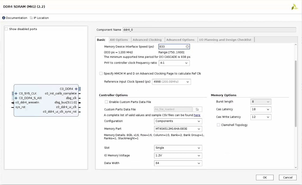 DDR4 IP Configuration Interface
4.2.1.2 XDMA IP Core
XDMA IP core (DMA for PCI Express) is a hardware IP provided by AMD (Xilinx), full name “DMA Subsystem for PCI Express”. It is a dedicated engine for high-speed data transfer between FPGA and host memory, enabling ultra-high-speed, low-latency transmission with minimal CPU intervention.
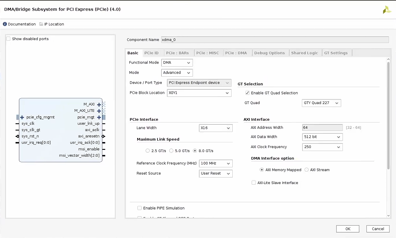 XDMA IP Core Configuration
In this project, we use GEN3 x16 mode, so select 8GT/s rate and x16 lane width in IP configuration.
4.2.1.3 DMA Stream Interface
In this project, DMA data width is 256bit.
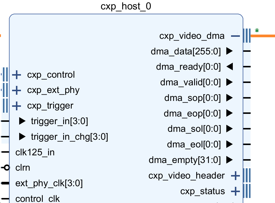 DMA Stream Interface Block Diagram
The video output interface is defined as a DMA bus. Port descriptions are shown in the table below.
Table 4-1 Video Stream DMA Interface
| Signal Name | I/O | Width | Description |
|---|---|---|---|
| dma_clk | Input | STREAMS | DMA stream clock. |
| dma_data | Output | 32*STREAM_WORDSxSTREAMS | DMA stream data. |
| dma_empty | Output | WIDTH_O(1)xSTREAMS | DMA empty indicator, marks the last transfer of a frame. |
| dma_valid | Output | STREAMS | DMA data valid signal; low suspends transmission. |
| dma_ready | Input | STREAMS | DMA data ready signal. |
| dma_sop | Output | STREAMS | Start of frame indicator. |
| dma_eop | Output | STREAMS | End of frame indicator. |
| dma_sol | Output | STREAMS | Start of line indicator. |
| dma_eol | Output | STREAMS | End of line indicator. |
1. The WIDTH_O is defined as Log2(4 x STREAM_WORDS)
Video DMA Stream is a universal video stream interface. How are data and pixels mapped?
When STREAMS=1 and STREAM_WORDS=4, dma_data width is 128bit, data arrangement as follows:
- If the device transmits 8bit pixels, the output stream through the DMA bus contains 8bit pixel data, total 16 pixels per clock cycle. Pixel 0 uses dma_data[7:0], pixel 1 uses [15:8], and so on.
- If the device transmits 10/12/14/16bit pixels, the decoded stream consists of 16bit pixel data, total 8 pixels per clock cycle. Data is stored in the lower 10/12/14/16 bits. For example, for 12bit pixels, pixel 0 uses dma_data[11:0], pixel 1 uses [27:16], and so on.
DMA_SOP and DMA_EOP indicate frame start and frame end.
DMA_SOL and DMA_EOL indicate line start and line end.
DMA_EMPTY indicates the number of empty bytes in the last transfer of a frame. In this design, it is always 0 when data is valid; data is internally packed.
 Figure 4-3 Video DMA timing
Figure 4-3 Video DMA timing (14-bit pixel example, 58 pixels shown)
1. dma_valid and dma_data assert on rising edge of dma_clk; dma_ready high → transfer completes.
2. dma_sop and dma_sol assert when dma_valid and dma_ready are both high → frame start.
3. Transfer pauses if dma_ready is invalid; buffered by internal FIFO.
4. Transfer resumes when dma_ready asserts again.
5. dma_valid high = active; low = pause.
6. Transfer resumes when dma_valid is high again.
7. dma_eop and dma_eol high → frame end. dma_empty=12 means 12 invalid bytes, 4 valid bytes (2 pixels for 14bit).
8. dma_eop low → frame complete.
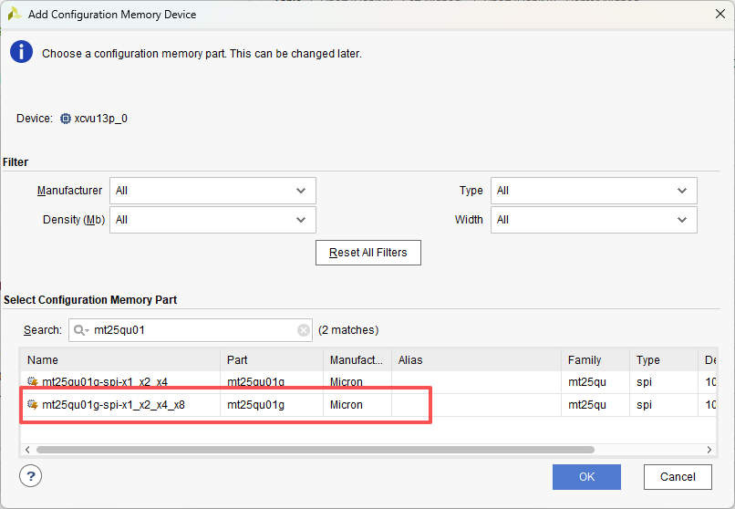
4.2.2 Firmware Flash
Note: The demo project uses SPI×8, which is very different from SPI×4. SPI×8 requires two different files to be burned into two FLASH devices. After generating the BIT file, use it to generate two MCS files. Click Tools → Generate Memory Configuration File….
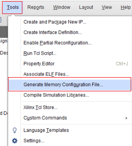
Enter the MCS file generation window.
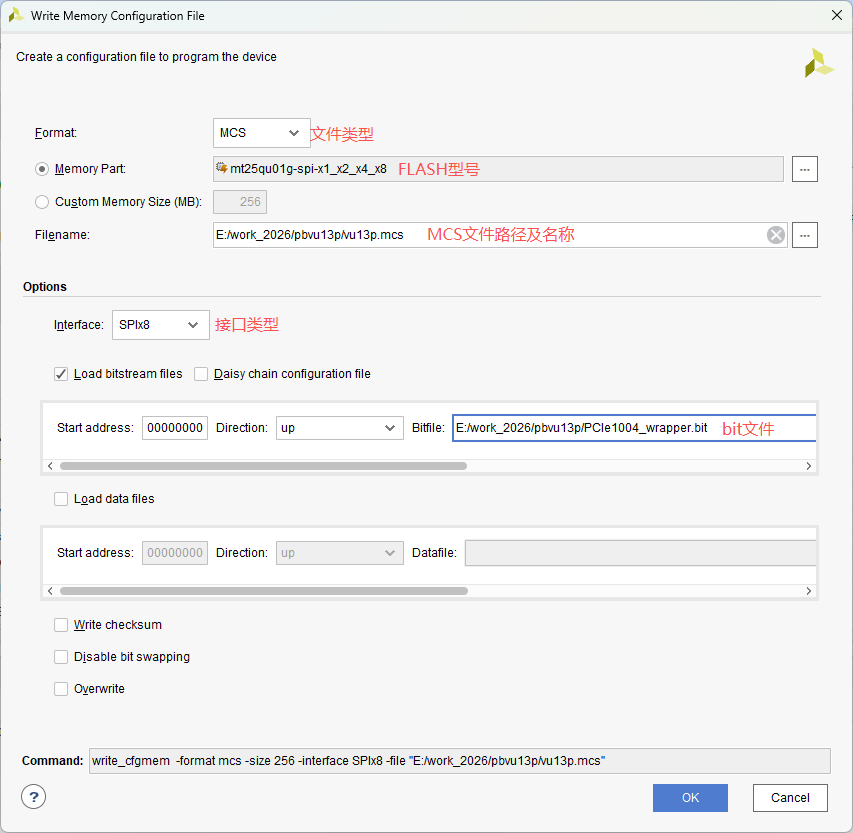 MCS File Generation Interface
Select MCS format, select the FLASH model marked in the figure.
 Flash Model Selection Screenshot
Select SPI×8 interface, load the BIT file, click OK. The MCS file is generated.
Then burn the MCS files. Select the FLASH model, load the generated MCS files, click OK.
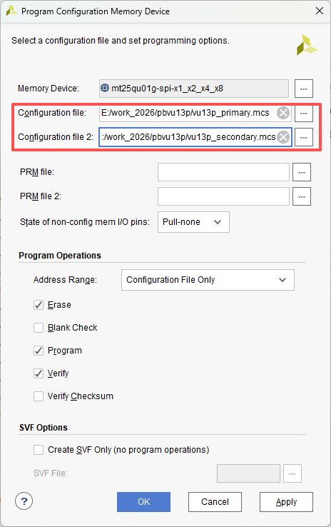
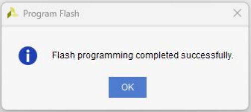
After programming completes, power off the board, remove the programmer, then power on again. The firmware in FLASH will boot automatically.
4.3 ImaGrab
ImaGrab is a Windows/Linux GUI client designed by Xingce Electronics. It supports CoaXPress device discovery, parameter configuration, real-time preview and image capture without programming. Suitable for on-site debugging, system integration and teaching. For more details, see Img-Grab User Manual: https://img-grab.com/filedownload/3000793
4.3.1 Main Functions
- Scan and enumerate all connected PCIe cards and attached cameras;
- Supports GenICam standard parameter tree (exposure time, gain, trigger mode, ROI, etc.);
- Real-time image display (supports zoom);
- Manual / automatic capture control;
- PoCXP power switch and current monitoring;
- External I/O trigger configuration (direction, level, routing);
- Log export and firmware upgrade entry.
4.3.2 Interface Layout
ImaGrab uses a modular design. The main interface is divided into six functional areas. Each area function is as follows:
| Area | Name | Function |
|---|---|---|
| 1 | Menu Bar | Provides global functions such as File (save image, export log), View (layout), Settings (language, unit), Tools and Help (version info, user manual). |
| 2 | Device List | Displays PCIe-1004 cards and connected CXP cameras; supports device switching. |
| 3 | Interface & Device Info | Model, SN, firmware, link status (CXP-12/6), PoCXP current. |
| 4 | Image Preview | Real-time display with FPS, bandwidth, resolution; supports zoom, pseudo-color, grid. |
| 5 | Feature Tree Panel | Complete GenICam parameters (width, height, pixel format, trigger, I/O). |

Figure 4-4 ImaGrab Main Interface
4.3.3 ImaGrab Quick Start Guide
ImaGrab client supports zero-configuration setup. Below are the basic steps to connect a camera and capture images:
- Launch the Software
Double-click the desktop shortcut ImaGrab.exe to launch the client.
- Scan for and Connect to the Camera
Click the [Refresh Devices] button in the toolbar. The system will automatically scan for acquisition cards in the PCIe slots and attached CoaXPress cameras. Double-click the target camera in the device list (Area 2). The software will automatically establish a connection, load the GenICam XML description file, and display all configurable parameters in the feature tree panel (Area 5).
- Configure Camera Parameters
You can view or modify parameters in the feature tree on the right, such as:
Width / Height: Set ROI;
ExposureTime: Adjust exposure time;
TriggerMode: Select trigger mode (Off/On);
LineSelector + LineMode: Configure External I/O functions.
Modified parameters usually take effect immediately (some parameters require stopping acquisition before modification).
- Start Image Acquisition
Click the [Continuous Acquisition] button in the toolbar to start the real-time image stream.
The image will be displayed in the preview window (Area 4), with real-time frame rate (FPS), resolution and other information shown.
- Save Images or Video
Single-frame Save: Click the [Save Image] button above the preview window. Supported formats include BMP, JPG, PNG;
Video Recording: Click the [Record Video] button. Data will be saved in raw binary (.bin) format, retaining complete image header information for later playback or analysis.
- Video Playback
In the menu bar, select [File] → [Create Playback System].
Load the saved .bin video file. You can then perform frame-by-frame playback, parameter review, and image export in ImaGrab.
4.3.4 GUI Examples
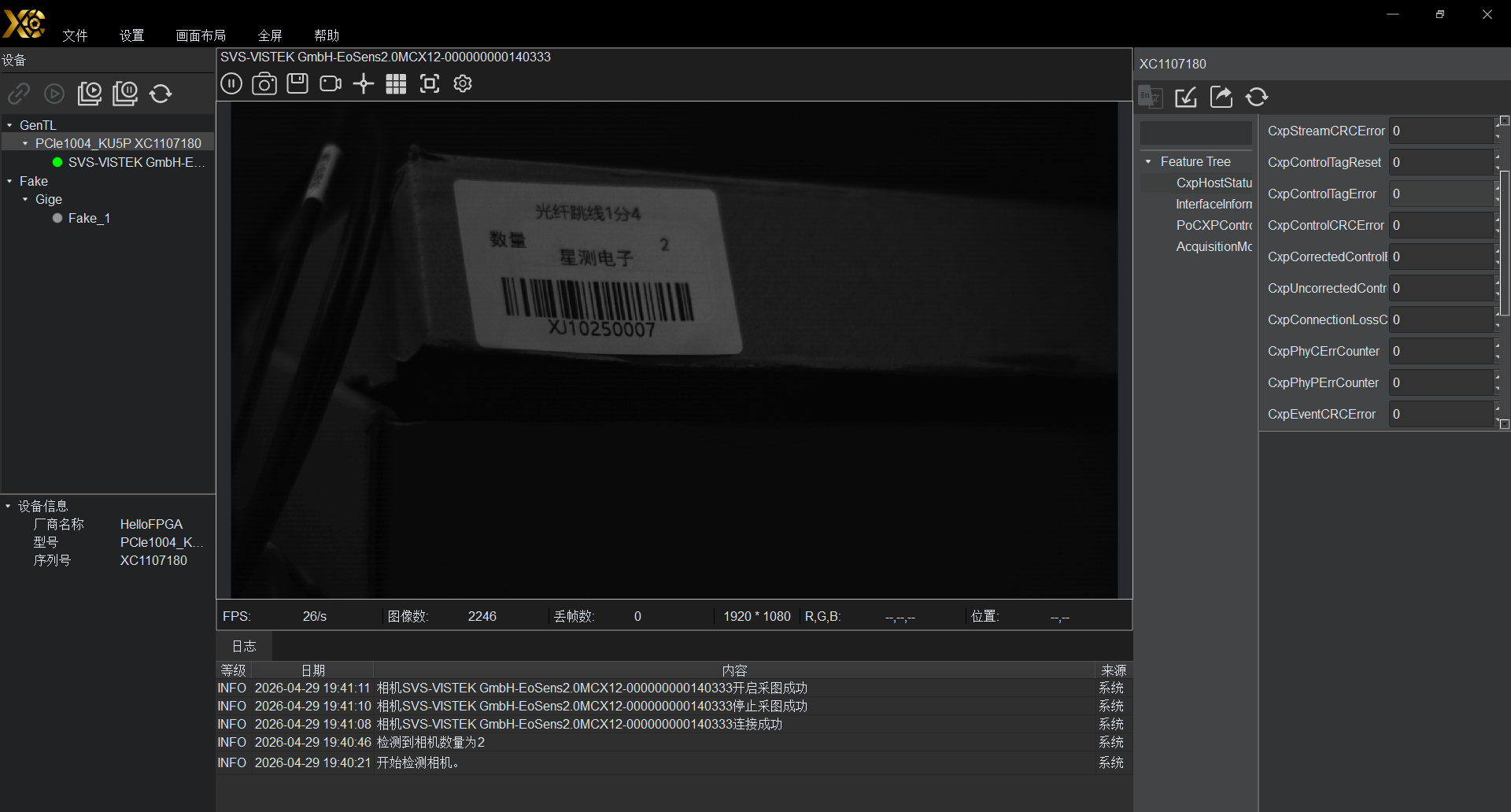
Figure 4-5 ImaGrab VU13P Test Image 1
Insert the board into PCIe, connect CXP camera via CXP cable. After firmware boots, use the host software to capture and display images from the camera through the VU13P card.
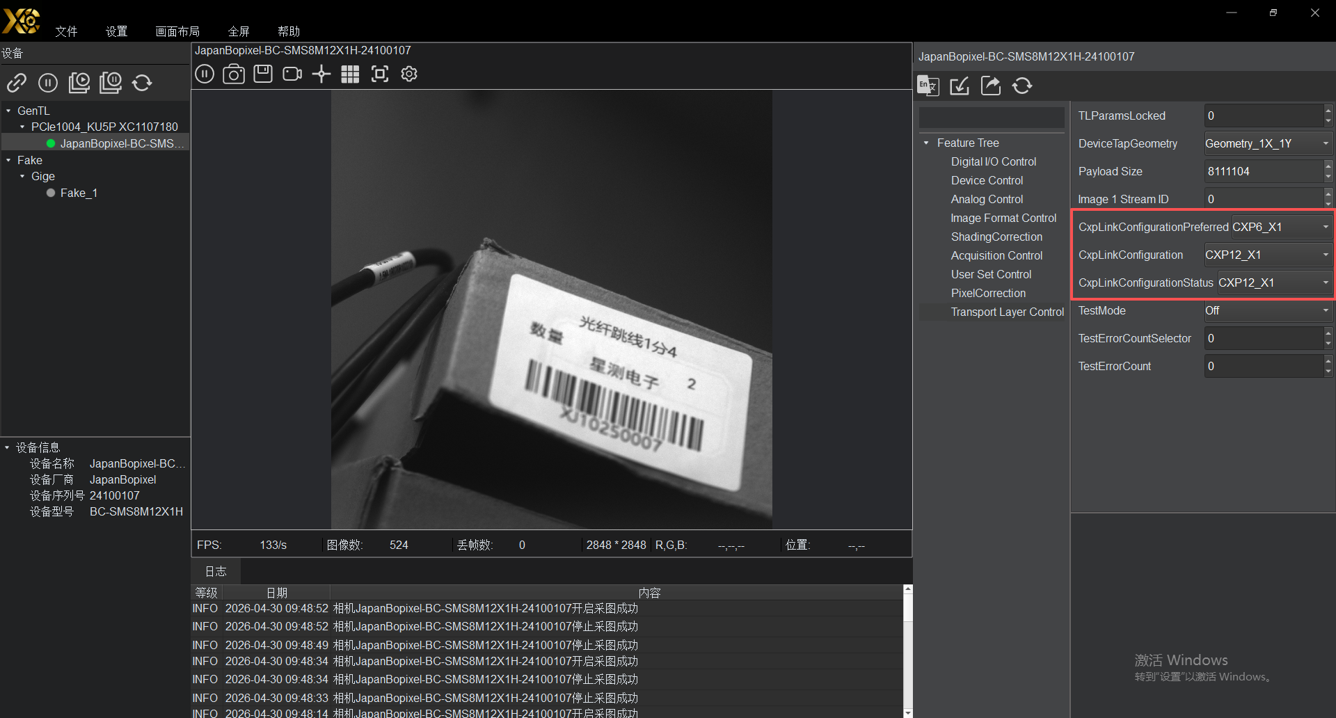
Figure 4-6 ImaGrab Test Image 2
Speed configuration: up to 12.5G. Go to Transport Layer Control: CxpLinkConfigurationPreferred (read-only recommended speed), CxpLinkConfiguration (configurable), CxpLinkConfigurationStatus (actual speed). Refresh after changing speed.
GPIO control: Not exported in current firmware; requires secondary development.
Annex A:References
1. CoaXPress JIIA CXP-001-2021
