KU5P Development Board New Highlight Experiment | Camera Link High-Speed Image Acquisition
Camera Link Test Experiment
1 Experiment Content
In this example, the XILINX serial-to-parallel conversion module is used to implement the data reception and serial-to-parallel conversion of Camera Link. The common method is to use a dedicated serial-to-parallel conversion chip to realize serial-to-parallel conversion. This experiment is directly implemented by Xilinx FPGA without a dedicated serial-to-parallel conversion chip, which can greatly save IO resources.
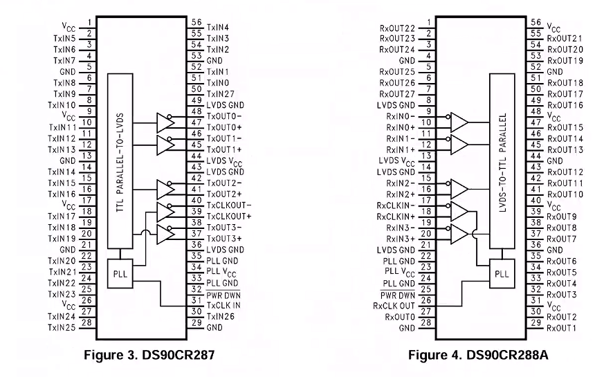
As shown in the figure below: DS90CR288 is a serial-to-parallel conversion chip, which converts the input differential LVDS serial signal into a 27-bit parallel signal output. This requires 27 FPGA IOs to correspond to it, which consumes a large number of IO pins.
2 Experiment Environment
Vivado 2022.2
Hello-FPGA-KU5P Development Board with Hello-FPGA CL-FULL-FMC Subcard
PCIe4005 Camera Link Analog Camera Source
Camera Link Industrial Camera Cable
3 Experiment Principle
3.1 Introduction to Camera Link
Camera Link is a high-performance digital image transmission protocol designed for industrial image processing applications, issued by the Automated Imaging Association (AIA). Based on Channel Link (LVDS) technology, it aims to solve the standardization problem of large-data-volume transmission between high-speed CMOS/CCD cameras and image acquisition cards. Camera Link adopts a parallel-to-serial mechanism to achieve extremely high bandwidth with very few connections. Its basic components include:
(1) Camera end: Converts parallel image data into serial low-voltage differential signaling (LVDS) for transmission.
(2) Cable: Special 26-pin double-shielded cable to ensure the anti-interference ability of signals at high frequencies.
(3) Acquisition card end: Receives LVDS signals and restores them to parallel image data for processing by FPGA or processor
In this experiment, the Hello-FPGA-KU5P Development Board acts as the acquisition card end
3.2 Camera Link Communication Protocol
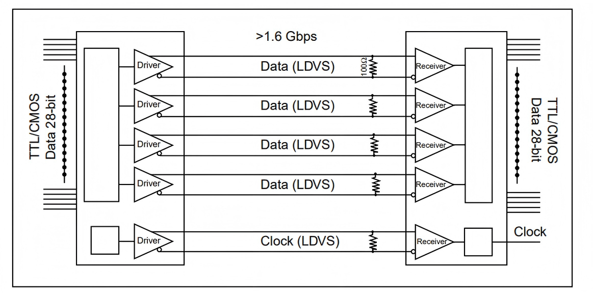
Channel Link consists of a driver and a receiver. The driver receives 28 single-ended data signals and one single-ended clock signal. Data is serialized at a ratio of 7:1, and four data streams and one dedicated clock signal are transmitted through five LVDS pairs. The receiver receives four LVDS data streams and LVDS clock signals, and then transmits 28-bit data and one clock signal to the circuit board
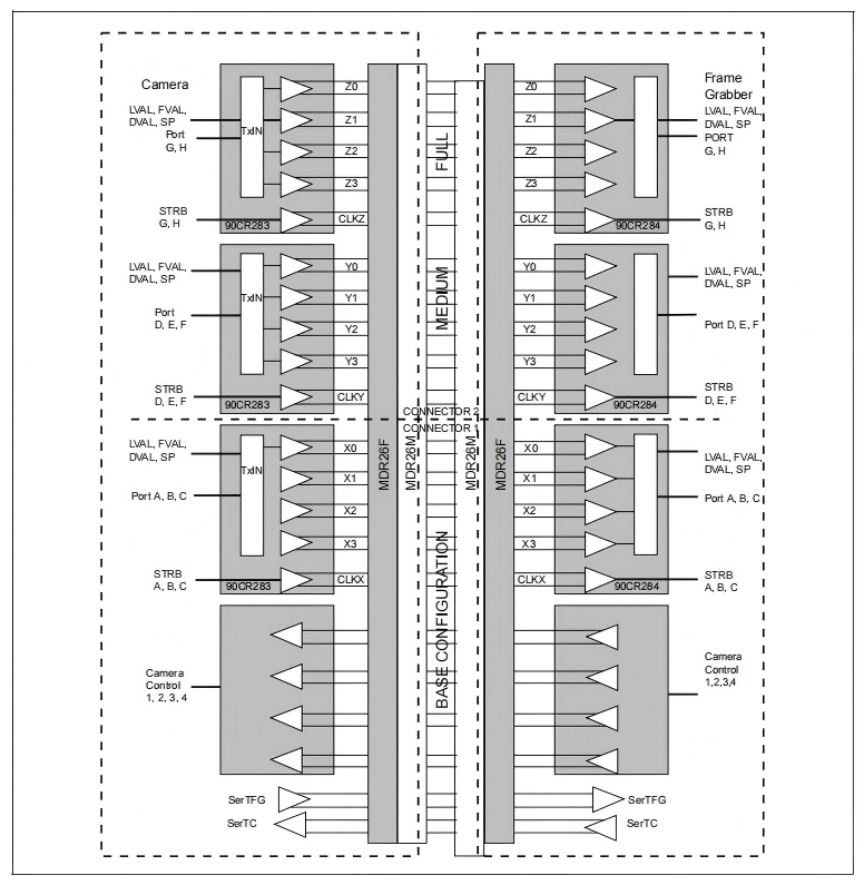
The Camera Link interface has three configurations. Due to the 28-bit capacity limitation of a single Channel Link chip, some cameras may require multiple chips to transmit data efficiently. The naming rules for various configurations are as follows:
(1) Base mode: Uses a single channel, including 24-bit image data and 4-bit synchronization signals.
(2) Medium mode: Uses two channels, the data width is increased to 48 bits, 4-bit synchronization signals.
(3) Full mode: Uses three channels, the data width reaches 64 bits, 4-bit synchronization signals.
Synchronization signals: During data transmission, four key synchronization signals are sent along with the data bits to define the effective range of a frame of image:
(1) FVAL (Frame Valid): Frame valid signal.
(2) LVAL (Line Valid): Line valid signal.
(3) DVAL (Data Valid): Data valid signal.
(4) Spare: Spare signal, usually reserved.

4 Program Design
4.1 Overall Program Introduction
The function of this program is that the FPGA receives and parses the high-speed video stream signals of the external Camera Link (supports Base/Medium/Full modes), completes LVDS 1:7 deserialization and protocol bit decomposition. Meanwhile, the core focus of this experiment observation is: directly capture the count values of the synchronization signals (LVAL, FVAL, DVAL) of the first 24 frames of the video through the internal counting statistics circuit and large-scale ILA (Integrated Logic Analyzer), so as to accurately verify the correctness and integrity of high-speed video interface data transmission.
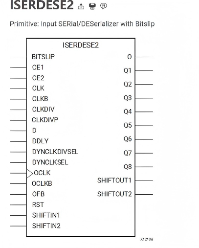
4.2 rx_channel_1to7 and rx_clkgen_1to7 Modules
These modules together implement a complete high-bandwidth LVDS video data deserializer transceiver for the Camera Link protocol. Each pair of LVDS differential data lines transmits 7 bits of data per pixel clock cycle.
The rx_clkgen_1to7 module receives the accompanying differential pixel clock (clkin_p/n), generates a high-speed sampling clock, performs clock calibration and phase alignment on the data bit stream, and searches for clock pattern matching (e.g., 7'b1100011). The rx_channel_1to7 module relies on the input clock to synchronously perform deserialization of multi-channel LVDS input signals (datain_p/n). By instantiating the device-specific ISERDES resources, the ultra-high-speed serial data stream is finally converted into a low-speed parallel data bus data_out, and the low-frequency pixel clock px_clk is restored and output for subsequent processing.
4.3 CameraLink_bit_allocation_rx Module
This module implements a combinational logic mapping circuit that remaps the deserialized parallel data stream (data_in is 84 bits wide in Full mode, i.e., 3 channels × 4 groups of lines × 7 bits/line) into the pixel data format of the video port specified by the standard Camera Link protocol.
Core processing flow:
(1) Mode matching and selection: Judge the current link mode (1 for Base, 2 for Medium, 3 for Full) through N (i.e., CAMERA_LINK_MODE parameter), and use the generate statement to generate allocation logic on demand.
(2) Bit allocation analysis:
Base mode (Chip X signal): Intercept the corresponding data bit segment in data_in, extract the line valid (xLVAL), frame valid (xFVAL), data valid (xDVAL) control signals of the video, and re-splice and allocate the pixel bytes to PortA, PortB, PortC ports according to pin and protocol requirements.
Medium mode (Chip Y signal): Add a fixed bit offset (X*7), continue to parse the second channel of synchronization and control signals yLVAL/FVAL/DVAL beyond the basic mode, and intercept the corresponding bytes to allocate to PortD, PortE, PortF ports.
Full mode (Chip Z signal): Add double bit offset (X*2*7) to obtain the remaining control signals zLVAL/FVAL/DVAL and the corresponding PortG, PortH data ports.
4.4 CameraLink Module
This module is the working center of Camera Link link reception and processing: First, it instantiates the IDELAYCTRL specific to the hardware series, and uses the 300MHz reference clock to precisely calibrate the delay of each input pin of the receiving channel to ensure the alignment of the data eye diagram. Dynamically synthesize the required differential input lines (datain_p and datain_n) according to the configuration parameters. Summarize the three groups of differential signals X, Y, Z scattered on the pins and extract the parallel data bus data_out through the rx_channel_1to7 instance. Then, feed it as input to the CameraLink_bit_allocation_rx instance to complete the final video protocol layer extraction operation, and expose the effective pixel output port, clock and status flag to the upper layer.
4.5 counter Synchronization Signal Counting Module
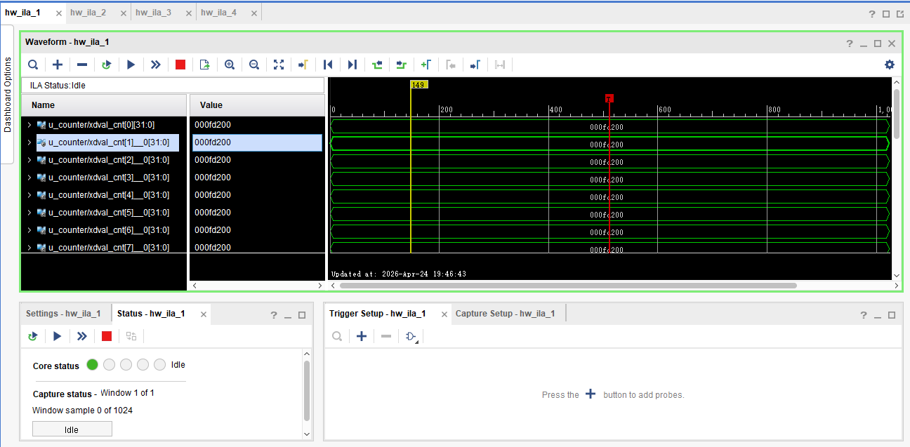
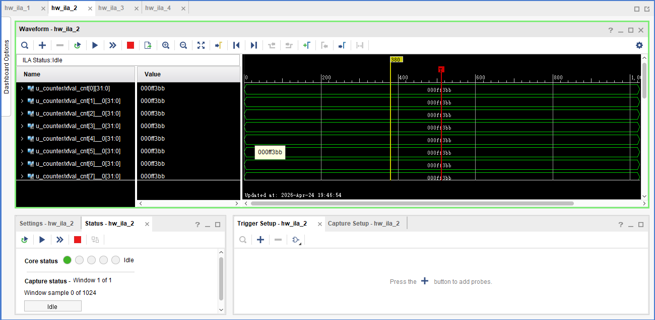
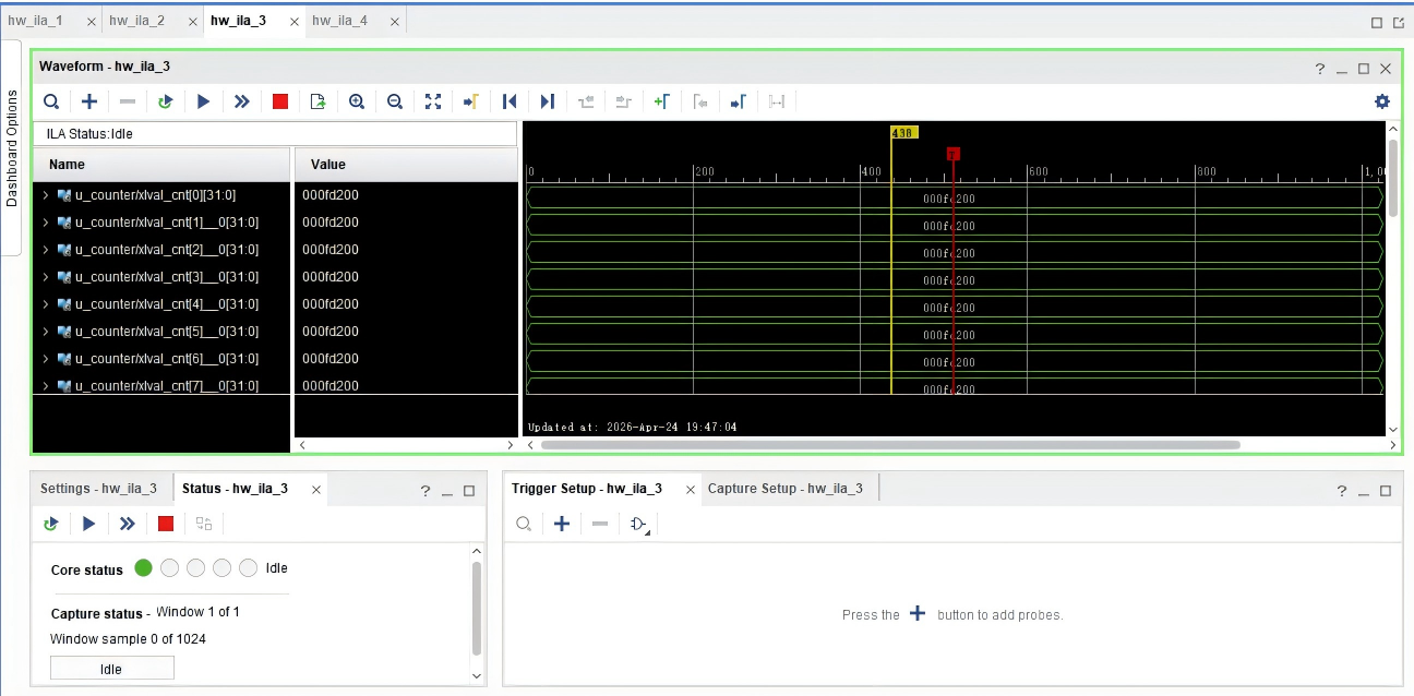
The key to the successful observation and verification of this experiment lies in this module. This module discretely counts the three major synchronization flags LVAL/FVAL/DVAL extracted by deserialization under the pixel clock of each channel:
Frame edge trigger and tracking: Detect the rising edge of the frame valid signal (xFVAL_pos) through register beat, use the counter frame_cnt to track the total number of received frames, and limit the statistics to only the first 24 frames (frame_cnt <= 24).
Pixel-level fine statistics (two-dimensional array recording): The code creates a register array with a depth of 24 for storing:
xlval_cnt [0:23]: Record the total number of clock cycles when LVAL is at high level in each frame (representing the number of lines/vertical resolution);
xfval_cnt [0:23]: Record the total number of clock cycles when FVAL is at high level in each frame;
xdval_cnt [0:23]: Record the total number of data valid cycles when DVAL is at high level in each frame (representing the total amount of effective pixel load).
Continuously accumulate +1 during the valid period of each frame. Through this hardware statistics method, it can intuitively quantify whether the timing output by Camera Link matches the expected frame resolution parameters.
4.6 top Top Module and ILA Online Observation System
While integrating the above logic, the core design of the top module is to insert multiple sets of ILA (Integrated Logic Analyzer) for observation and proof of experimental results:
Bottom connection waveform monitoring (ila_clout): The ILA instantiated in top.v has its probes directly connected to the video clock, LVAL/FVAL/DVAL and Port output channels after deserialization and recombination. Its function is to allow experimenters to identify the edge alignment relationship of signals and whether the parallel image data has been stably output at the oscilloscope waveform level.
24-frame array statistics monitoring (ila_xdval_cnt, ila_xlval_cnt, etc.): Inside counter.v, dedicated ILA cores with high bandwidth (32 bits) and multi-channel (with 24 probe ports) are instantiated for the count values of DVAL, LVAL, etc.
Experiment observation method: The experimenter does not need an external actual display and host computer software, only needs to power on online, open Vivado Hardware Manager to connect to the ILA trigger board. Directly read the independent count value cache of the 24 frames from probe0 to probe23. As long as the values such as xlval_cnt output by these counters are exactly stable and equal to the known resolution specifications of the target camera (e.g., no missing lines, no misaligned pixels), it proves that the Camera Link acquisition and data recovery are all correct, and the experiment obtains the most powerful hardware convincing experimental verification conclusion.
5 Board Verification
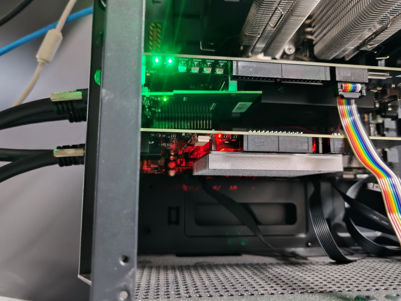
First, insert the Hello-FPGA CL-FULL-FMC subcard into the Hello-FPGA-KU5P Development Board, then insert the Hello-FPGA-KU5P Development Board and the PCIe4005 Camera Link Analog Camera Source into the PCIe slot of the motherboard, and then connect the two boards with a Camera Link industrial camera cable
Then burn the bit file into the board. After burning, the software will automatically open the ila interface

Then press key4 on the KU5P to reset the device, and capture the data of ila1 directly without setting a trigger
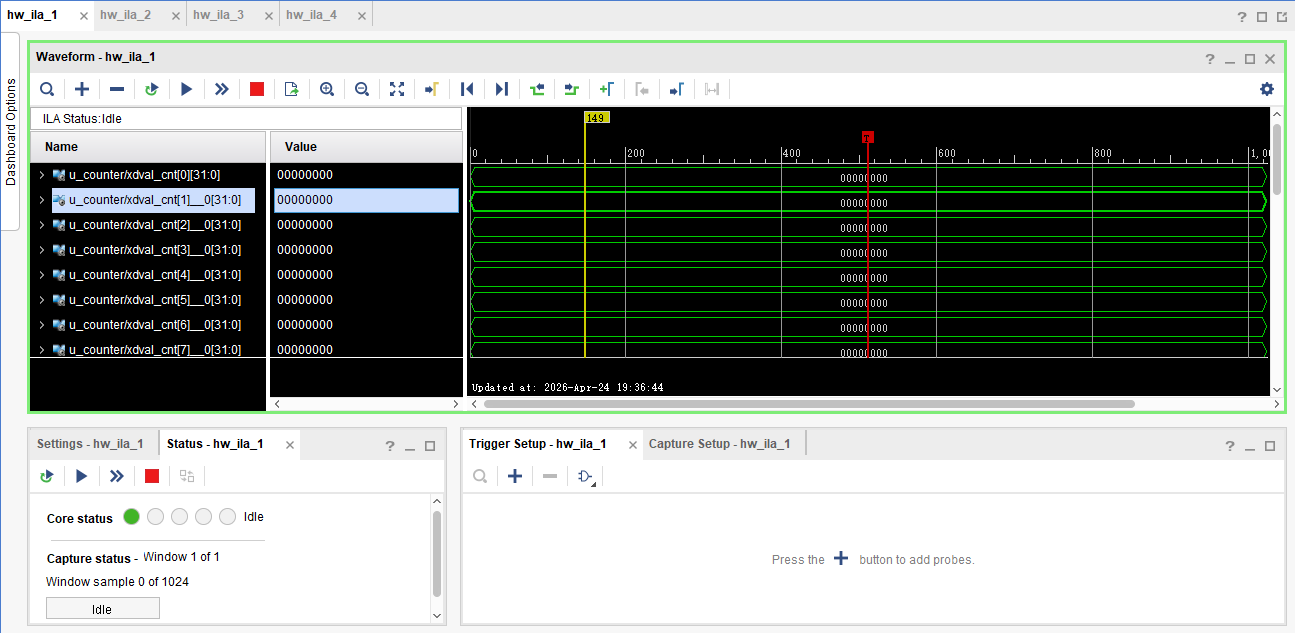
It is found that all data are 0 at this time, indicating that the counter has been reset.
Open the interface of ila4, set the trigger to the rising edge of the frame valid signal, which means capturing once per frame, and set the number of trigger windows to capture multiple trigger results, set to 30
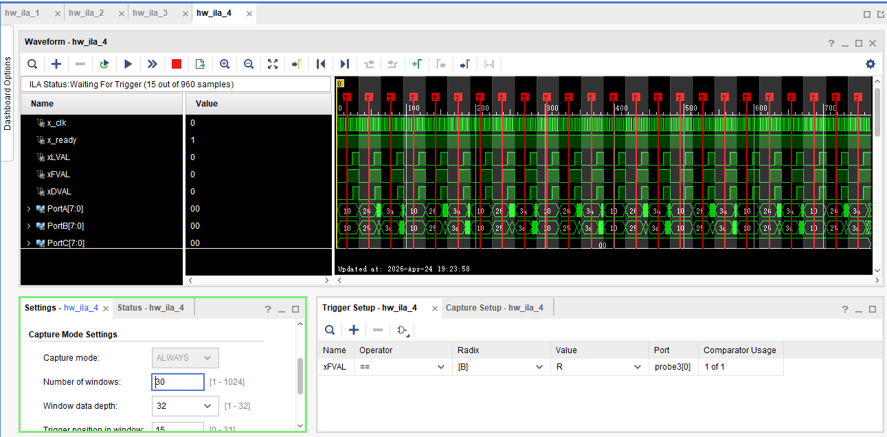
Then start capturing and wait for the analog camera source to send data
Open the host computer software of PCIe4005 and send 24 frames of pictures
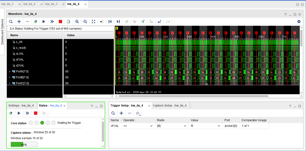
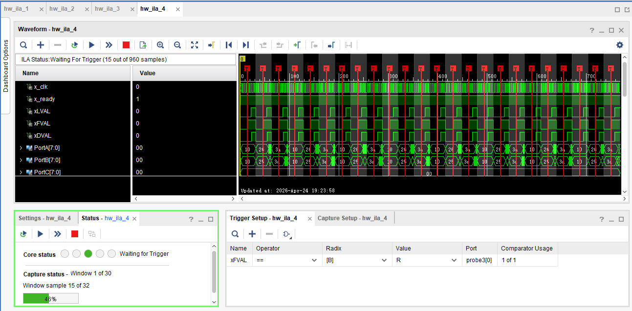
It is observed that the capture status changes from 1 to 25, indicating that 24 rising edges of the frame valid signal have been captured
Then stop the trigger, and you can see that the interface of ila4 has been triggered 24 times
At this time, open the interfaces of ila1, ila2, and ila3 respectively, and capture directly without setting the trigger signal to obtain the counter results after the KU5P receives these 24 pictures. It is observed that the data of each frame is the same